2 layers50 × 18 mm
Majestouch stm32
mbtech-nl/majestouch-stm32
Drop-in replacement controller for the full-size Filco Majestouch: STM32F072, QMK with NKRO over USB. KiCad 9 board, hand-solderable.
20 parts2MIT

 project802/kunlun
Technical information about the Kunlun keyboard
Kunlun STM32 MCU Board is an open-source printed circuit board by project802, from the project802/kunlun repository on GitHub. It is a 2-layer board of 40 × 40 mm with 40 parts on 58 nets, routed with 206 tracks and 42 vias.
It is built around the STM32F072CBT6, AP2112K-3.3 and USBLC6-2SC6, with the 10129383-908001ALF, SMAJ5.0CA and USB4105-GF-A among its other parts. Its parts include 12 capacitors, 9 connectors, 7 resistors, 3 ICs and 1 diode. It belongs with the keyboards and input and microcontroller boards boards and the STM32 boards of this library.


This repository contains documentation for repairing and upgrading the Kunlun keyboard from YDKB / KBDfans.
My Kunlun stopped functioning after one too many ESD strikes approximately 3 years into ownership. The journey to create this documentation started because I wanted to bring my keyboard back to life, and there were no replacement parts.
The failure mode presented as "ghost" key presses. Pressing one key anywhere on the PCB with the failed shift register(s) would register many or all (depending on the duration of the keypress) keys from the same PCB.
As I began the repair, I realized that the design was not something I had seen before, nor was it one commonly seen in the mechanical keyboard community (for good reason, see the section below on shift registers). It is remarkably simple, and therefore remarkably easy to diagnose and repair.
I have designed a replacement MCU board based on an STM32F072. For more information, see the mcu board redesign folder. Improvements include ESD support, an upgraded processor that allows for enabling all Vial features, and a speaker.
During this process, I also ported the original firmware written by YDKB to the latest version of Vial. QMK has grown a lot since Kunlun was introduced, so it required some optimization and feature set choices to be made to fit within the microcontroller constraints.
My port can be found here: https://github.com/project802/vial-qmk
A prebuilt image can be found in the prebuilt binaries folder.
To update the firmware:
Microcontroller - Atmel Mega32U4-AU (datasheet)
A basic 8-bit microcontroller that is commonly seen in keyboards that support QMK. KBDfans used the TQFP44 package and placed it on a small PCB just for the usb interface, power supply, and microcontroller.
Kunlun uses the internal oscillator and only operates at 8 MHz, as VCC is connected to a regulated 3.3V supply and 16 MHz would require > 4.5V.
Shift Registers - 74HC595 (datasheet)
When is a 74HC595 not a 74HC595? When its the one used on this keyboard. Apparently, FM decided to usurp the identifier and make something that is almost the same, but isn't. It uses open drain outputs (instead of push/pull) and also doesn't have either a latch clock nor output enable.
The part is available on LCSC.
This drove almost the entirety of why I went on the reverse engineering journey. The faulty shift registers were replaced with standard parts, and the keyboard had the same failure symptoms. After much head scratching, I figured they had to be open drain outputs and searched Google to find a Facebook post and an EEVblog thread that confirmed my suspicion.
The matrix is scanned entirely using only 3 GPIO.
Serial clock and data are sent to the left and right PCB in parallel.
All switches on the right PCB have one side tied to a unique shift register output, and the other to PB2.
All switches on the left PCB have one side tied to a unique shift register output, and the other to PB3 through a 2.2kOhm resistor.
The shift registers on each PCB are run in serial so that shifting the test bit goes through each output sequentially.
Pressing a key acts as a jumper between its corresponding shift register output with the appropriate microcontroller input. If the shift register output is open drain (the bit is set to one), voltage at the microcontroller is not affected and remain logically high. If the shift register output is driven low (the keypress test bit, zero) then it will pull down the appropriate microcontroller input.
Scanning
That's it. It is arguably slower than a typical row/col matrix, but it can still be completed in short order (optimized to approximately 350 microseconds in my port) so it doesn't present any meaningful lag as the USB HID interface runs on a 1 millisecond interval. As a result, the stock and ported firmware restrict the scan rate to no faster than 1 kHz.
The photos in this section display the behavior of stock firmware. My ported firmware has different waveforms and sequences.
In my case, the microcontroller appeared to have full function so my focus was on the left and right PCBs.
The right PCB was the closest to where the final ESD strike occurred so that is also where I started checking. There was no visible physical damage, so the first tests were to probe the various pins on the shift registers.
Starting with the first register in the chain, U24, verify inputs on pins 11 (clock) and 14 (data). You should see something similar to below.
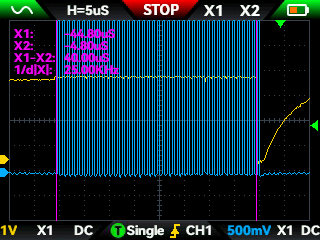
The data (yellow trace) can be seen driving low, clocked in, and slowly rising due to the weak pull-up.
Next, check pin 9 to make sure the IC is shifting the bit out and into the next one in the chain. In my case, this was part of the failure mode. It was not outputting anything but low so it was clocking in zeros to the next IC, so on and so forth, causing everything to look like it was pressed at the same time.
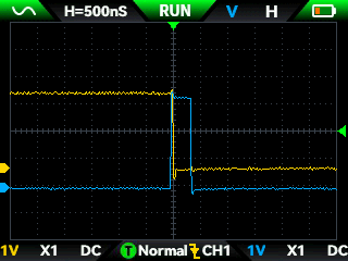
Check the outputs of the shift register to make sure they are switching between open drain and driving low. You will need to press a key to connect the output to the pull-up within the micro, otherwise it will look like its driving low the entire time. It isn't! I also had this failure mode where the lines were driving low. It seems my IC had a dead data input internally and was always reading zeros so it latched those to the outputs and shifted it into the next in line.
A key pressed with its shift register output (yellow) and the bit clock (blue) is below.
| Qty | Value | Footprint | References |
|---|---|---|---|
| 4 | 100nF | Capacitor_SMD:C_0603_1608Metric | C1, C2, C4, C8 |
| 4 | 1uF | Capacitor_SMD:C_0603_1608Metric | C7, C10, C11, C12 |
| 4 | 5002 | TestPoint:TestPoint_Keystone_5000-5004_Miniature | J4, J5, J6, J7 |
| 2 | 22 | Resistor_SMD:R_0603_1608Metric | R1, R2 |
| 2 | 4.7uF | Capacitor_SMD:C_0603_1608Metric | C3, C5 |
| 2 | 5.1k | Resistor_SMD:R_0603_1608Metric | R4, R5 |
| 2 | 5001 | TestPoint:TestPoint_Keystone_5000-5004_Miniature | J8, J9 |
| 1 | 0532610671 | Connector_Molex:Molex_PicoBlade_53261-0671_1x06-1MP_P1.25mm_Horizontal | J1 |
| 1 | 100 | Resistor_SMD:R_0603_1608Metric | R7 |
| 1 | 10129383-908001ALF | Connector_PinHeader_2.54mm:PinHeader_2x04_P2.54mm_Vertical_SMD | J2 |
| 1 | 10k | Resistor_SMD:R_0603_1608Metric | R3 |
| 1 | 10nF | Capacitor_SMD:C_0603_1608Metric | C6 |
| 1 | 1M | Resistor_SMD:R_1206_3216Metric | R6 |
| 1 | 1nF | Capacitor_SMD:C_1206_3216Metric | C9 |
| 1 | 500mA | Fuse:Fuse_1206_3216Metric | F1 |
| 1 | AP2112K-3.3 | Package_TO_SOT_SMD:SOT-23-5 | U2 |
| 1 | KMR231NG ULC LFS | Button_Switch_SMD:SW_Push_1P1T_NO_CK_KMR2 | SW1 |
| 1 | MountingHole_Pad | MountingHole:MountingHole_2.2mm_M2_Pad | H1 |
| 1 | SMAJ5.0CA | Diode_SMD:D_SMA | D1 |
| 1 | STM32F072CBT6 | Package_QFP:LQFP-48_7x7mm_P0.5mm | U1 |
| 1 | SolderJumper_3_Bridged12 | Jumper:SolderJumper-3_P1.3mm_Bridged12_RoundedPad1.0x1.5mm | JP1 |
| 1 | Speaker | Buzzer_Beeper:Buzzer_CUI_CPT-9019S-SMT | LS1 |
| 1 | USB4105-GF-A | Connector_USB:USB_C_Receptacle_GCT_USB4105-xx-A_16P_TopMnt_Horizontal | J3 |
| 1 | USBLC6-2SC6 | Package_TO_SOT_SMD:SOT-23-6 | U3 |
The 37 most common of 40 parts.
It measures 40 × 40 mm and has 2 copper layers, 1.6 mm thick.
40 parts, built around the STM32F072CBT6, AP2112K-3.3, USBLC6-2SC6 and 10129383-908001ALF. The full list of its parts is on this page, with links to each part's symbol and footprint where PCBKit's library has them.
From the project802/kunlun repository on GitHub, at the commit this page was made from: the board is mcu board redesign/kicad/Kunlun STM32 MCU Board.kicad_pcb and its schematic kicad/Kunlun.kicad_sch. PCBKit opens the board in the browser, with nothing to install.
Its repository states no licence, so its author keeps all rights: ask project802 before reusing the design.
mbtech-nl/majestouch-stm32
Drop-in replacement controller for the full-size Filco Majestouch: STM32F072, QMK with NKRO over USB. KiCad 9 board, hand-solderable.


SharbelMarshi/txrx-optical-communication-kicad
A Free-Space Optical Communication link KiCad project

danstiner/embedded
+-----------+-----+----------------------+--------------------+------------------------------------------------------------------------+ | Reference | Qty | Value | Part Number | Footprint |…

RaviKachhwaha/RUDRAKINUXIS-Lite
It is a high-performance 600W (20V–25.2V 6S) FOC BLDC ESC for UAVs & robotics. Powered by STM32G431 CORDIC MCU, it features 16 AWG wire-reinforced 2oz copper pads for motor/power, an integrated flight controller bus…


