Skip to the content
PCBKitNew board
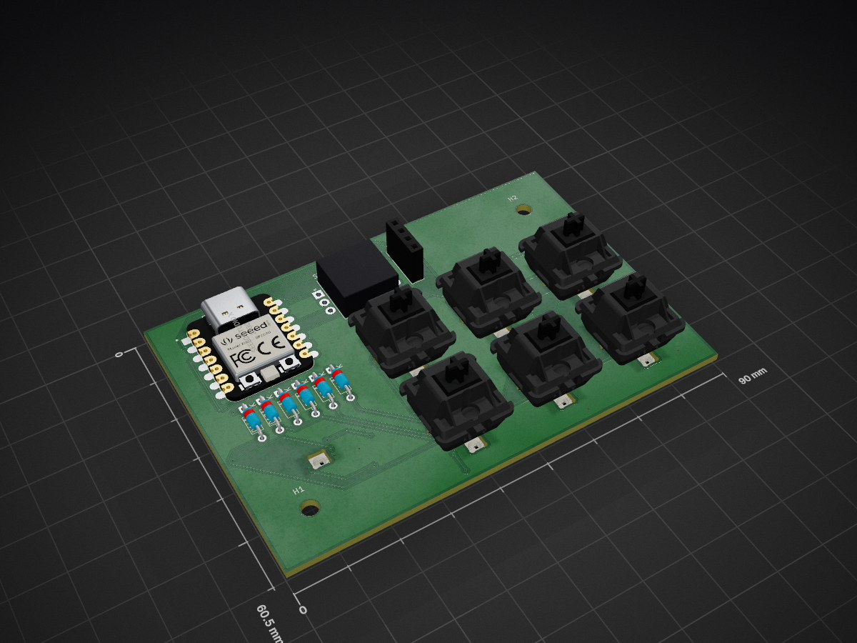
2 layers90 × 60.5 mmMypad, the printed circuit board in 3D

I made my very own macropad!

Size
90 × 60.5 mm
Copper layers
2
Thickness
1.6 mm
Parts
31
Nets
27
Pads
111
Tracks, vias
455, 34
Pours
1
Routed
Yes
KiCad
KiCad 10.0 (file 20260206)
Created
15 Aug 2026
Updated
18 Aug 2026

Overview

Mypad is an open-source printed circuit board by prodevmod, from the prodevmod/mypad repository on GitHub. It is a 2-layer board of 90 × 60.5 mm with 31 parts on 27 nets, routed with 455 tracks and 34 vias.

It is built around the WS2812B. Its parts include 13 diodes, 7 capacitors, 7 switches, 1 IC and 1 connector. It belongs with the keyboards and input boards and the RP2040 boards of this library.

Main components

1

README

README.md

WELCOME TO MYPAD

BROUGHT TO YOU BY Alexandros Rosario Morabito the 3rd

Picture of My Hackpad (in Cad)

image image

Made in fusion 360.


Picture of schematic

Schematic made in KiCad! image


Picture of PCB

PCB also made in Kicad! image


BOM

  • seeed XIAO RP2040
  • 6x 1N4148 Diodes
  • 6x MX-Style switches
  • 1x EC11 Rotary encoder
  • 1x 0.91 inch OLED display
  • 6x white blank DSA keycaps
  • 7x SK6812 MINI-E LEDs
  • 4x M3x10mm screws
  • 2x M3x5mm screws
  • 6x M3x5mx4mm heatset inserts
  • 7x Capacitor Ceramic 0.1uF 50 Volts X7R 0805 Hand Solder => $0.02 – $0.36 USD
  • 1x 3D printed case
  • 1x Custom PCB => $2.00 Before Shiping

A Few thoughts on the HACKPAD journey

  • It was mad cool and I want to give a big thx to HACKCLUB (search it up) and its community (that I am now a part of) for Helping me
  • I didnt know anything about firmware/PCB designing or cad and it shows, but this was a chance to gain insight by getting my hands dirty and I am glad for all the mistakes I learned from
  • I was very frustrated at times (like I am not a genius this is to much for my 15 yo brain)
  • I think thats it (I hope I get funded)
  • You will find a QMK Overview in Mypad\Firmware

Oh and some footage of me designing everything

Me Me

Parts

31
QtyValueFootprintReferences
7C_SmallCapacitor_SMD:C_0805_2012MetricC1, C2, C3, C4, C5, C6, C7
7WS2812Bfootprints:SK6812MINI-E_fixedD5, D6, D7, D8, D10, D11, D12
6DDiode_THT:D_DO-35_SOD27_P7.62mm_HorizontalD1, D2, D3, D4, D13, D14
6SW_Push_45degMX_Solderable:MX-Solderable-1USW2, SW3, SW4, SW5, SW6, SW7
2MountingHoleMountingHole:MountingHole_3.2mm_M3H1, H2
1OLED_DISPLAYConnector_PinHeader_2.54mm:PinHeader_1x04_P2.54mm_VerticalJ1
1RotaryEncoder_SwitchRotary_Encoder:RotaryEncoder_Alps_EC11E-Switch_Vertical_H20mmSW1
1Seeed Studio XIAO RP2040footprints:XIAO-Generic-Hybrid-14P-2.54-21X17.8MMU1

Questions

How big is the Mypad PCB?

It measures 90 × 60.5 mm and has 2 copper layers, 1.6 mm thick.

What parts does the Mypad use?

31 parts, built around the WS2812B. The full list of its parts is on this page, with links to each part's symbol and footprint where PCBKit's library has them.

Where can I download the Mypad KiCad files?

From the prodevmod/mypad repository on GitHub, at the commit this page was made from: the board is PCB/mypad.kicad_pcb and its schematic PCB/mypad.kicad_sch. PCBKit opens the board in the browser, with nothing to install.

Can I use the Mypad design in my own project?

Its repository states no licence, so its author keeps all rights: ask prodevmod before reusing the design.

Similar boards

  • 4 layers99 × 53.3 mmPSLab, the printed circuit board in 3D

    PSLab

    fossasia/pslab-hardware

    PSLab Hardware Design and Schematics https://pslab.io

    199 parts1.7kApache-2.0
  • 2 layers26 × 30 mmMicrocontroller, the printed circuit board in 3D

    Microcontroller

    FrameworkComputer/ExpansionCards

    Reference designs and documentation to create Expansion Cards for the Framework Laptop

    34 parts1.1kCC-BY-4.0
  • 4 layers82.6 × 82.5 mmJumperless2, the printed circuit board in 3D

    Jumperless2

    Architeuthis-Flux/Jumperless

    A jumperless breadboard

    208 parts914
  • 2 layers95.3 × 161.9 mmDfh badge, the printed circuit board in 3D

    Dfh badge

    tanaes/whopping_Voron_mods

    135 parts787GPL-3.0
  • 2 layers42.8 × 28.8 mmMM Skirt, the printed circuit board in 3D

    MM Skirt

    PrintersForAnts/Micron

    If you want to purchase full kits there are 3 available (Kits are slowly updating to R1 hardware just make sure to double check the included hardware in your kit and if you have any questions reach out in the discord)

    11 parts741GPL-3.0
  • 2 layers149.6 × 127.1 mmErgodash, the printed circuit board in 3D

    Ergodash

    omkbd/ErgoDash

    keyboard

    187 parts732MIT
  • 2 layers285.5 × 95 mmReviung46 ver1 1, the printed circuit board in 3D

    Reviung46 ver1 1

    gtips/reviung

    The REVIUNG41 is 41-key column staggered keyboard.

    119 parts517MIT
  • 2 layers177.7 × 144.5 mmCOMM PANEL, the printed circuit board in 3D

    COMM PANEL

    jrsteensen/OpenHornet

    OpenHornet 1:1 F/A-18C Simulator Repository

    275 parts431