2 layers115 × 88 mm
 princessbrynn/TempMonitor
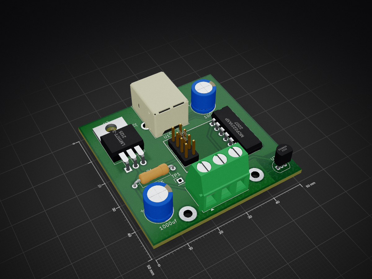
TempMonitor is an open-source printed circuit board by princessbrynn, from the princessbrynn/TempMonitor repository on GitHub. It is a 2-layer board of 50 × 50 mm with 13 parts on 17 nets, routed with 65 tracks and 0 vias.
It is built around the DS18B20 and LM1117T-3.3. Its parts include 4 ICs, 2 capacitors, 2 connectors and 1 resistor. It belongs with the ESP8266 boards of this library.


| Qty | Value | Footprint | References |
|---|---|---|---|
| 2 | 1000uf | Capacitor_THT:CP_Radial_D8.0mm_P3.80mm | C1, C2 |
| 1 | 4.7K | Resistor_THT:R_Axial_DIN0309_L9.0mm_D3.2mm_P12.70mm_Horizontal | R1 |
| 1 | DS18B20 | Package_TO_SOT_THT:TO-92_Inline | U3 |
| 1 | ESP-01v090 | ESP8266:ESP-01 | U1 |
| 1 | LM1117T-3.3 | Package_TO_SOT_THT:TO-220-3_Horizontal_TabDown | U2 |
| 1 | MCP2221AxP | Package_DIP:DIP-14_W7.62mm | U4 |
| 1 | Screw_Terminal_01x03 | TerminalBlock_Phoenix:TerminalBlock_Phoenix_MKDS-1,5-3_1x03_P5.00mm_Horizontal | J1 |
| 1 | TestPoint | Connector_PinHeader_2.54mm:PinHeader_1x01_P2.54mm_Vertical | TP1 |
| 1 | USB_B | Connector_USB:USB_B_OST_USB-B1HSxx_Horizontal | J2 |
The 10 most common of 13 parts.
It measures 50 × 50 mm and has 2 copper layers, 1.6 mm thick.
13 parts, built around the DS18B20 and LM1117T-3.3. The full list of its parts is on this page, with links to each part's symbol and footprint where PCBKit's library has them.
From the princessbrynn/TempMonitor repository on GitHub, at the commit this page was made from: the board is TempMonitor.kicad_pcb and its schematic TempMonitor.kicad_sch. PCBKit opens the board in the browser, with nothing to install.
Its repository states no licence, so its author keeps all rights: ask princessbrynn before reusing the design.


DRWJSCHMIDT/T41
This is the repository for the officially released V10, V11, and V12 versions of the T41 Software Defined Transceiver hardware and kits.


ceteras/PicoLVDS
Tested with B089AW01-V.0 and HSD089IFW1-A00-V1.0 on a breadboard. I'm sure it will work with other displays from old netbooks.
