2 layers132.1 × 45.7 mm
IPoS
peterheinrich/InternetOverSpaghetti
Transmitting IP packages over a pair of spaghetti thus demonstrating how media independent IP really is.
42 parts342

 PRESIT007/555-Timer-Delay-Off-Circuit
555 timer-based push-button relay timer designed in KiCad.
Delay off timer ckt is an open-source printed circuit board by PRESIT007, from the PRESIT007/555-Timer-Delay-Off-Circuit repository on GitHub. It is a 2-layer board of 79.2 × 37 mm with 14 parts on 13 nets, routed with 116 tracks and 0 vias.
It is built around the L7805 and BC547. Its parts include 3 capacitors, 2 resistors, 2 ICs, 2 connectors and 2 switches. It belongs with the home automation and IoT boards of this library.


A practical electronics learning project exploring delay-off timer operation, relay control, and PCB design using a 555 timer IC and KiCad.
This project is part of my learning journey as an Electrical Engineering student. The goal is to understand how a timer circuit works, how its components determine the delay, and how a circuit moves from a schematic to a PCB layout.
Important: Confirm the exact timing behavior and formula against the final schematic and practical test. The operation depends on how the 555 timer, trigger, RC network, and relay interface are connected.
A delay-off timer keeps a load operating for a defined period and then switches it OFF. Depending on the design, the delay may begin when a trigger is applied or when a control signal is removed.
In a relay-based circuit, relay contacts can switch a separate load. The relay's input polarity and the timer's output interface determine how the load behaves during the timing interval.
Confirm the exact sequence for this circuit against the schematic and practical test: what happens at power-up, when the button is pressed, and when the delay expires.
The 555 timer contains internal comparators, a latch, and a discharge transistor. These monitor the timing capacitor voltage and control the output state.
In a common monostable configuration:
The external circuit configuration determines whether this sequence matches the intended delay-off behavior.
A resistor-capacitor (RC) network sets the time required for the capacitor voltage to change.
For a conventional 555 monostable circuit, the approximate pulse duration is:
T ≈ 1.1 × R × C
Where:
This formula applies only to the corresponding monostable topology. Other 555 configurations can use different timing relationships. Actual timing varies with component tolerances, capacitor leakage, supply voltage, temperature, and circuit implementation.
Refer to the actual schematic and BOM.csv for confirmed values, quantities, footprints, and part numbers.
| Component | Purpose |
|---|---|
| 555 timer IC | Generates the timing response |
| Timing resistor(s) | Control capacitor charging or discharging rate |
| Timing capacitor | Stores charge and establishes the interval |
| Push button / trigger input | Initiates the timing sequence, according to the circuit |
| Relay or relay module | Switches the external load |
| Power supply and connectors | Provide power and circuit connections |
| PCB and footprints | Provide the physical circuit layout |
Verify all component values against the final schematic before assembly.
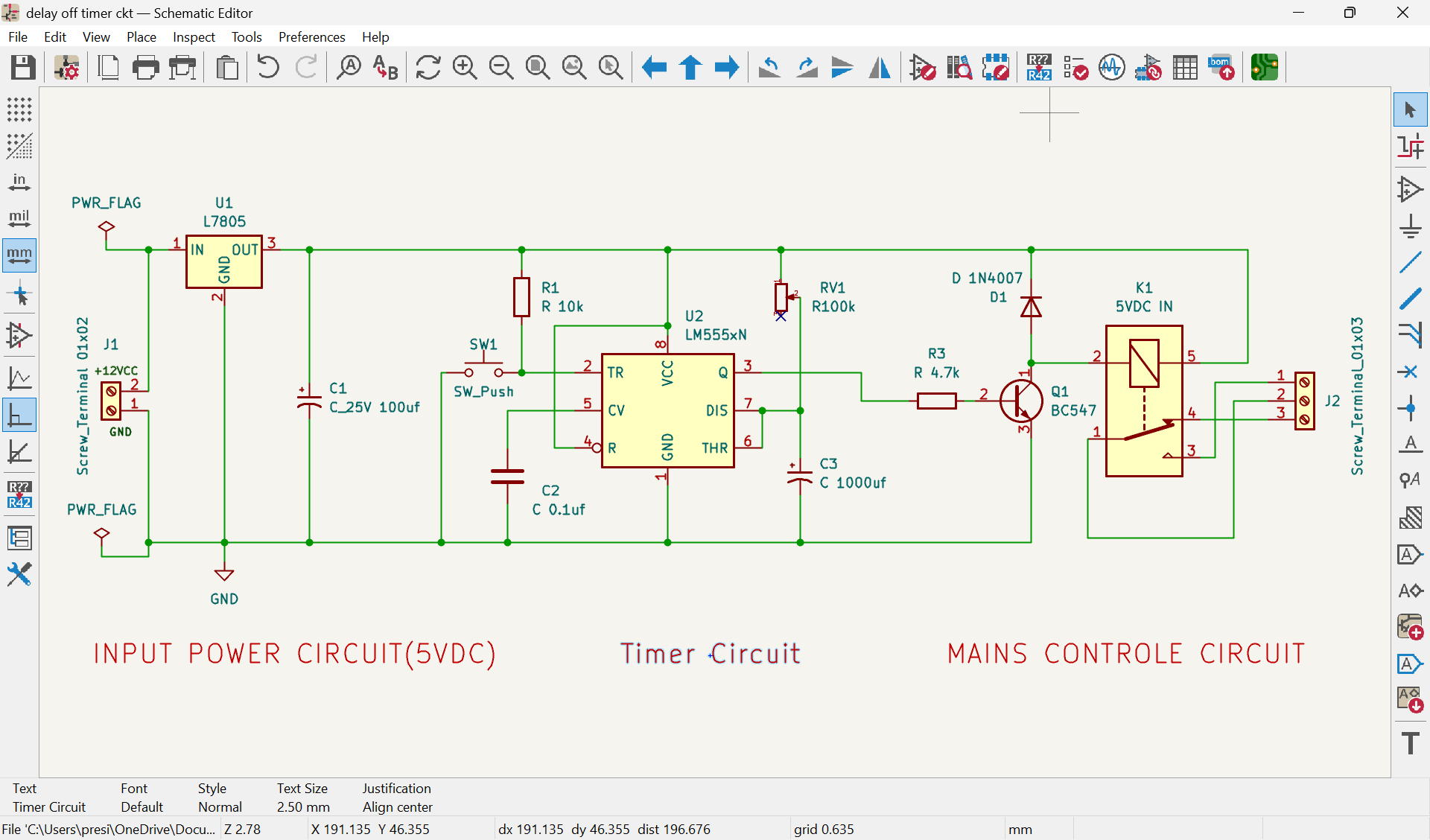
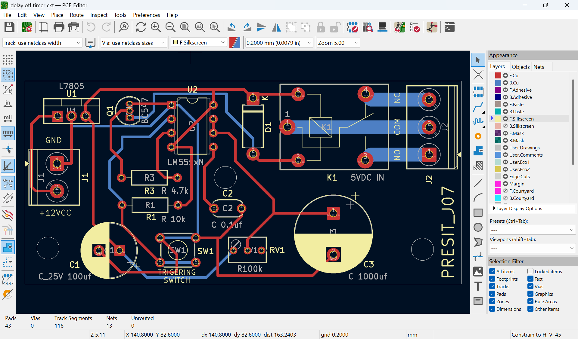
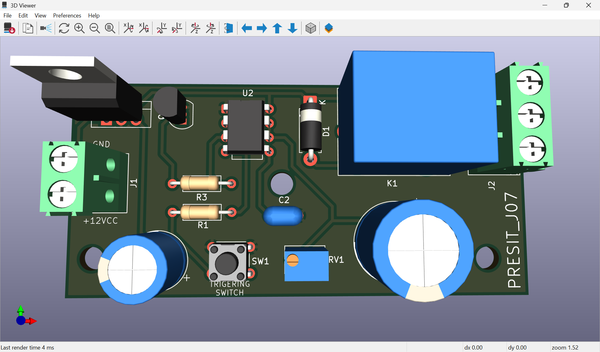
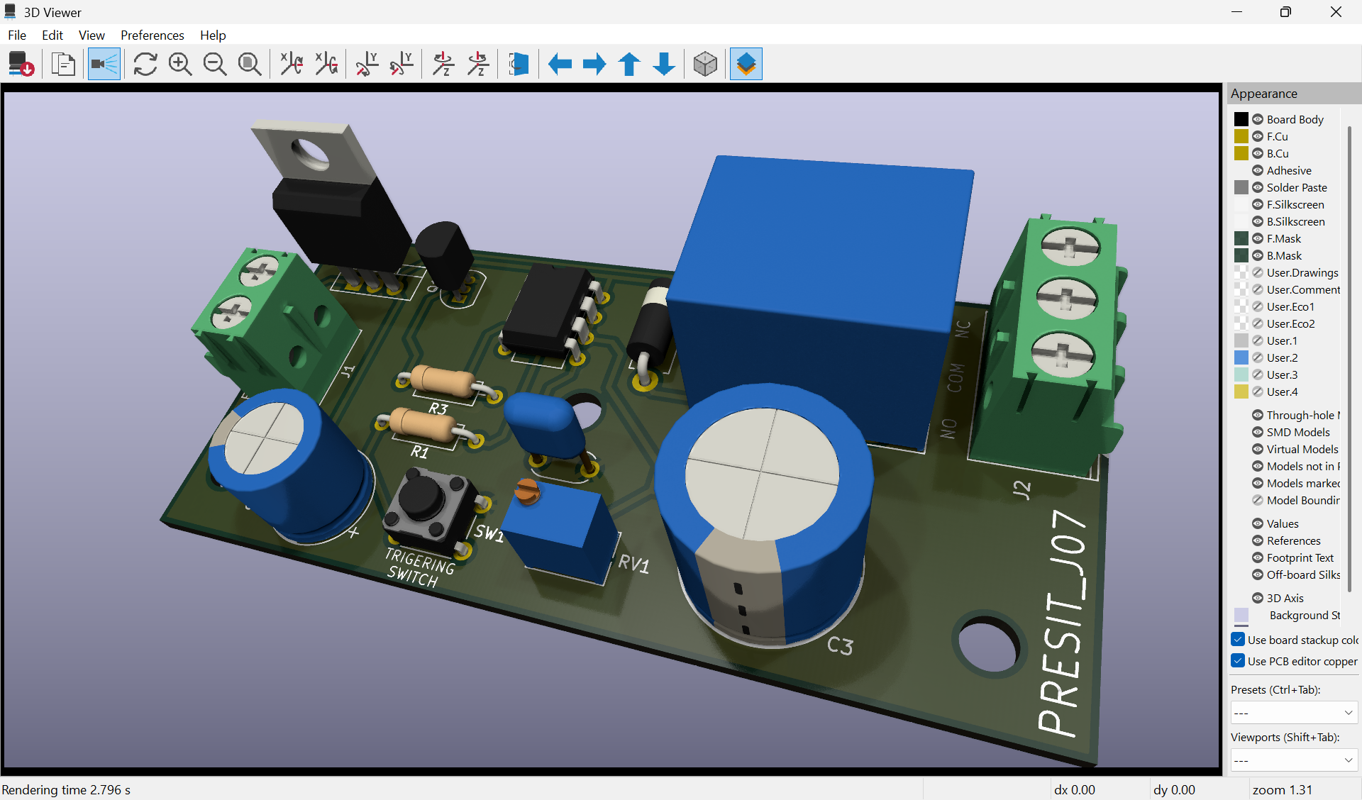
Update image paths if your repository uses different folders or filenames.
This is a suggested structure. Keep the paths consistent with the files uploaded to GitHub.
555-Timer-Delay-Off-Circuit/
├── README.md
├── schematic.pdf
├── BOM.csv
├── Gerber.zip
├── KiCad/
│   ├── delay off timer ckt.kicad_pro
│   ├── delay off timer ckt.kicad_sch
│   └── delay off timer ckt.kicad_pcb
└── Images/
    ├── schematic.png
    ├── pcb-layout.png
    ├── 1_pcb-3d.png
    └── 2_pcb-3d.png
.kicad_pro — KiCad project settings.kicad_sch — editable schematic.kicad_pcb — editable PCB layoutschematic.pdf — printable schematicBOM.csv — component listGerber.zip — manufacturing outputs, if it contains exported Gerber and drill files.kicad_pro file in KiCad.A useful experiment is to measure the delay several times, calculate the average, and compare it with the theoretical value from the correct circuit equation. Record differences and consider component tolerances and circuit topology.
Application suitability depends on the circuit ratings and tested behavior.
Through this project, I am learning to:
This project's hardware design files, including the KiCad schematic and PCB layout, are licensed under the CERN Open Hardware Licence Version 2 – Strongly Reciprocal (CERN-OHL-S-2.0).
You may use, study, modify, and redistribute the covered design files under the terms of this license. Modified versions of the covered hardware design must comply with its applicable reciprocal-sharing requirements.
See the full CERN-OHL-S-2.0 license for details.
Project type: Electrical Engineering · PCB Design · Analog Electronics · Timer Circuits · PCB Design
Design tool: KiCad
Purpose: Learning, experimentation, and documentation
| Qty | Value | Footprint | References |
|---|---|---|---|
| 1 | 5VDC IN | Relay_THT:Relay_SPDT_SANYOU_SRD_Series_Form_C | K1 |
| 1 | BC547 | Package_TO_SOT_THT:TO-92_Inline | Q1 |
| 1 | C 0.1uf | Crystal:Resonator-2Pin_W6.0mm_H3.0mm | C2 |
| 1 | C 1000uf | Capacitor_THT:CP_Radial_D14.0mm_P7.50mm | C3 |
| 1 | C_25V 100uf | Capacitor_THT:CP_Radial_D10.0mm_P3.80mm | C1 |
| 1 | D 1N4007 | Diode_THT:D_DO-15_P10.16mm_Horizontal | D1 |
| 1 | L7805 | Package_TO_SOT_THT:TO-220-3_Vertical | U1 |
| 1 | LM555xN | Package_DIP:DIP-8_W7.62mm | U2 |
| 1 | R 10k | Resistor_THT:R_Axial_DIN0207_L6.3mm_D2.5mm_P10.16mm_Horizontal | R1 |
| 1 | R 4.7k | Resistor_THT:R_Axial_DIN0207_L6.3mm_D2.5mm_P10.16mm_Horizontal | R3 |
| 1 | R100k | Potentiometer_THT:Potentiometer_Bourns_3266Y_Vertical | RV1 |
| 1 | SW_Push | Button_Switch_THT:SW_TH_Tactile_Omron_B3F-102x | SW1 |
| 1 | Screw_Terminal 01x02 | TerminalBlock_Phoenix:TerminalBlock_Phoenix_PT-1,5-2-5.0-H_1x02_P5.00mm_Horizontal | J1 |
| 1 | Screw_Terminal_01x03 | TerminalBlock_Phoenix:TerminalBlock_Phoenix_PT-1,5-3-5.0-H_1x03_P5.00mm_Horizontal | J2 |
It measures 79.2 × 37 mm and has 2 copper layers, 1.6 mm thick.
14 parts, built around the L7805 and BC547. The full list of its parts is on this page, with links to each part's symbol and footprint where PCBKit's library has them.
From the PRESIT007/555-Timer-Delay-Off-Circuit repository on GitHub, at the commit this page was made from: the board is KiCAD/delay off timer ckt.kicad_pcb and its schematic KiCAD/delay off timer ckt.kicad_sch. PCBKit opens the board in the browser, with nothing to install.
Its repository states no licence, so its author keeps all rights: ask PRESIT007 before reusing the design.
peterheinrich/InternetOverSpaghetti
Transmitting IP packages over a pair of spaghetti thus demonstrating how media independent IP really is.

telec16/modular-synth
Little side project, don't expect much updates.

ashishkumarpardeshi/DIY_Oxygen_Analyzer
This repository is for Design and Development of DIY Oxygen Analyzer Prototyping Board, Writing Code and Calibration.


bmatthieu3/clockdivider
A simple clock divider module made with an Atmega328p

ajackson2681/codex
The Codex is an attempt at an open-source, distraction-free writing device inspired somewhat by the AlphaSmart Neo (at least the display was).