2 layers103 × 30.5 mm

 pranavnasrani/PowerPad
My first MacroPad! Thanks to HackClub!
Hackpad is an open-source printed circuit board by pranavnasrani, from the pranavnasrani/PowerPad repository on GitHub. It is a 2-layer board of 59.8 × 74 mm with 9 parts on 15 nets, routed with 99 tracks and 12 vias.
Its parts include 7 switches, 1 IC and 1 connector. It belongs with the keyboards and input boards and the RP2040 boards of this library.
Hello! Welcome to my PowerPad GitHub repository! You will find all the details for my HackPad in this repository
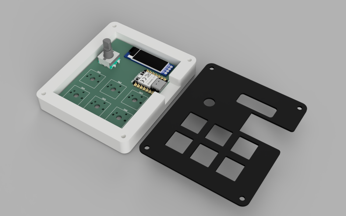
I use my computer a lot, especially for video editing, and a lot of coding/multitasking. I wanted to make a MacroPad that makes my life easier, helps me copy, paste, cut, undo, redo, all with ease. I use these shortcuts atleast 40 times a day, and having them just a buttons press away would be amazing. I also added a Rotary Encoder to control my volume (for my music), and possibly in the future, to scrub the video editing timeline. The OLED screen would display the current time and some cool graphics (have to work on that in the future through client based code).
This was not my first time using Fusion, however it was my first time doing PCB design, and I ran into a lot of problems with the footprints, and how to set up vias, but now I can confidently design simple PCBs.
Bill of Materials
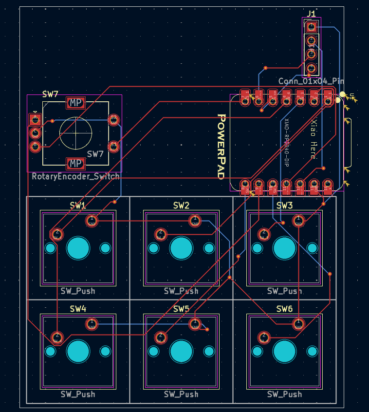
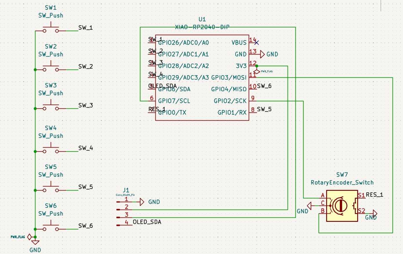
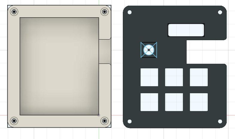
Case files (top and bottom case STEP files) can be found here
| Qty | Value | Footprint | References |
|---|---|---|---|
| 6 | SW_Push | Button_Switch_Keyboard:SW_Cherry_MX_1.00u_PCB | SW1, SW2, SW3, SW4, SW5, SW6 |
| 1 | Conn_01x04_Pin | Connector_PinHeader_2.54mm:PinHeader_1x04_P2.54mm_Vertical | J1 |
| 1 | RotaryEncoder_Switch | Rotary_Encoder:RotaryEncoder_Alps_EC11E-Switch_Vertical_H20mm | SW7 |
| 1 | XIAO-RP2040-DIP | OPL Lib:XIAO-RP2040-DIP | U1 |


FrameworkComputer/ExpansionCards
Reference designs and documentation to create Expansion Cards for the Framework Laptop

VoronDesign/Voron-Hardware
Cool Hardware designed by the Voron Design group

hackclub/OnBoard
💡 Join 1,000 teenagers and make your first PCB with a $100 grant!


adamws/kicad-kbplacer
KiCad plugin for automatic keyboard's key placement and routing
It measures 59.8 × 74 mm and has 2 copper layers, 1.6 mm thick.
9 parts. The full list of its parts is on this page, with links to each part's symbol and footprint where PCBKit's library has them.
From the pranavnasrani/PowerPad repository on GitHub, at the commit this page was made from: the board is pcb/hackpad.kicad_pcb and its schematic pcb/hackpad.kicad_sch. PCBKit opens the board in the browser, with nothing to install.
Its repository states no licence, so its author keeps all rights: ask pranavnasrani before reusing the design.