Skip to the content
4 layers70 × 70 mmFaikout, the printed circuit board in 3D

This is a cost optimize version of the original repo by RevK

Size
70 × 70 mm
Copper layers
4
Thickness
1.58 mm
Parts
37
Nets
46
Pads
167
Tracks, vias
195, 85
Pours
18
Routed
Yes
KiCad
KiCad 10.0 (file 20260206)
Created
3 Apr 2026
Updated
2 May 2026

Overview

Faikout is an open-source printed circuit board by Phiumi, from the Phiumi/ESP32-Faikout-CostOptimize repository on GitHub, published under the GPL-3.0 licence. It is a 4-layer board of 70 × 70 mm with 37 parts on 46 nets, routed with 195 tracks and 85 vias.

It is built around the ESP32-S3-MINI-1-N8, MPM3632CGQV-Z and 1N5819WS, with the H5VNT2B, S5B-EH(LF)(SN) and XL-3332RGBC-2812B among its other parts. Its parts include 9 capacitors, 6 resistors, 4 connectors, 3 diodes and 2 ICs. It belongs with the ESP32 boards of this library.

Main components

6

README

README.md

ESP32-Faikout (Cost-Optimized Re-design)

This repository contains a hardware redesign of the ESP32-Faikout, originally created by RevK.

This project is specifically optimized for JLC-PCB PCBA (Assembly service). The PCB dimensions are slightly larger, see the measurements below.
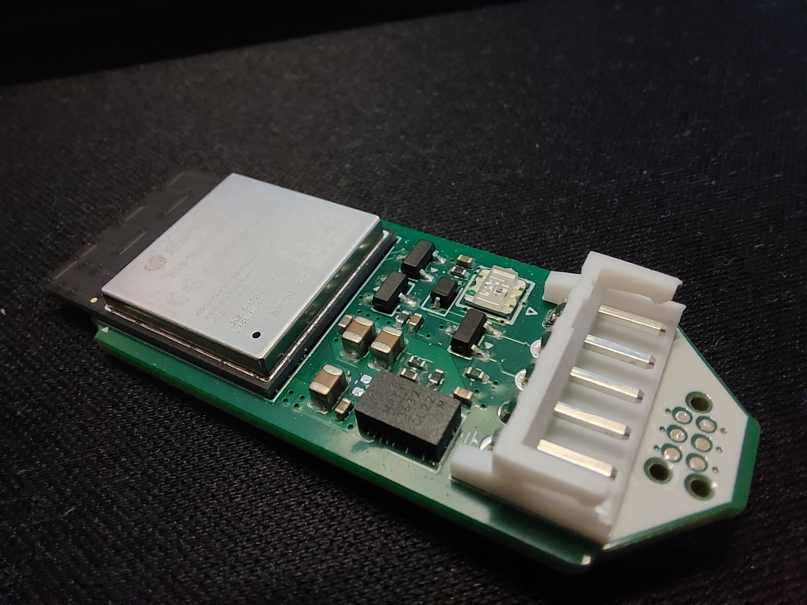
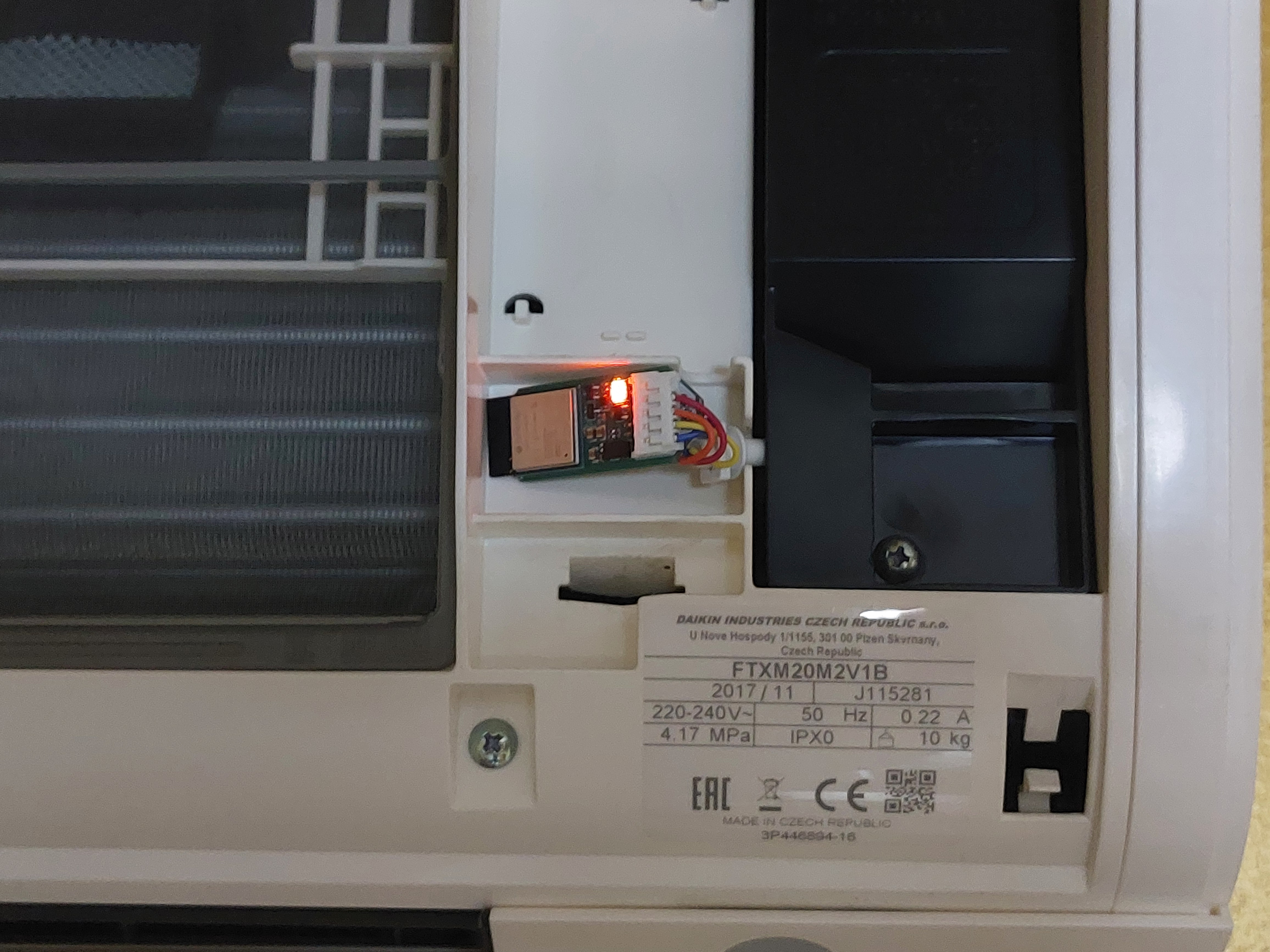
close-up in-action


🚀 Key Improvements in this Revision

This version introduces several technical optimizations to lower costs and improve manufacturing reliability:

  • Streamlined BOM: The Bill of Materials has been reduced from 17 lines to 13 lines, minimizing component variety and simplifying the assembly process.
  • JLC "Basic" Parts: Wherever possible, I have selected parts from the JLC Basic Library.
  • 4-Layer PCB Stackup: Upgraded from 2 layers to a 4-layer design. This allows for dedicated power/ground planes (still keeping low cost).
  • No 0201 Components: I have intentionally avoided 0201 footprints.
  • Revised Form Factor: The smallest module size is now 45mm x 16mm (up from 40mm x 16mm). This slight increase allows for the use of more common 0402 components.
  • Manufacturing Ready: The project is designed to be produced as a 70mm x 70mm panel (using JLC’s automatic panelization). This panel can then be broken down into various sizes as needed.
  • Avoid Baking: Replaced moisture-sensitive components from the original design to bypass the extra cost and time required for pre-assembly baking.
  • Ground-up PCB/SCH Redesign: The project features a reworked schematic and layout to support the updated BOM and manufacturing optimizations.

📜 Credits and Attribution

This project is a hardware derivative of the original ESP32-Faikout. All credit for the core concept, original schematics, and firmware goes to:

[NOTE]
This hardware revision is derived from commit 2c54c5f.


⚖️ License

This hardware redesign follows the licensing intent of the original project. Please consult the original repository for specific licensing terms regarding the firmware and base design.


Note for Users

If you are looking for the latest firmware updates or the full history of the project, please refer to RevK's original repository. This repo focuses specifically on the cost-optimized hardware layout and JLC-PCB manufacturing files.

How to order from JLC

Download the files from the releases, or generate the Gerber files yourself.
Go to the JLCPCB website, select “Get Instant Quote,” and upload the Gerber ZIP file.
You can flag "Specify Stackup" and select the "JLC04161H-3313", to have controlled impedance on the USB tracks.
Keep in mind that the ESP32-S3-MINI-1-N4R2 do not support economic assembly but only standard.
During the placement process, if you see a warning like the one below, simply click OK.
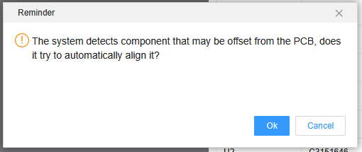
warning

The component placement should look like this, please check it carefully and ensure the orientation is correct. In most cases, JLCPCB will follow up with a confirmation email after reviewing the placement, asking you to verify that everything is correct. Review it thoroughly, as in my experience they may occasionally rotate diode packages by 180°.
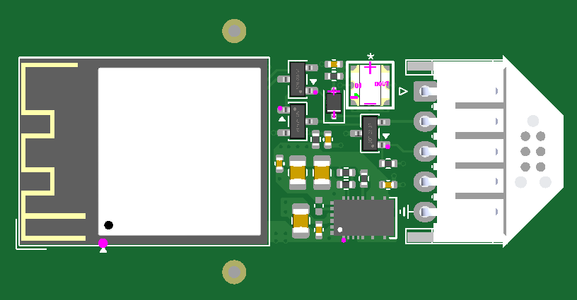
placing

V-cut issue

I usually prefer to place V-cuts on a separate layer and then ask JLCPCB in the remarks section to apply them. However, this time they ignored the request and did not perform the V-cuts, so I had to CNC the board myself. For your convenience, I’ve pushed a new commit where the V-cut layer is merged with the Edge Cuts layer, as required by JLCPCB’s documentation. I still recommend enabling the “Confirm Production File” option so you can review the files JLCPCB will send to production and verify that the V-cuts are included.

Parts

37
QtyValueFootprintReferences
9TestPointTestPoint:TestPoint_Pad_2.0x2.0mmTP1, TP2, TP3, TP4, TP5, TP6, TP7, TP8, TP9
51uFCapacitor_SMD:C_0402_1005MetricC1, C3, C5, C8, C9
310kResistor_SMD:R_0402_1005MetricR1, R2, R3
322uFCapacitor_SMD:C_0805_2012MetricC2, C6, C7
22N7002Package_TO_SOT_SMD:SOT-23Q1, Q2
2FiducialFiducial:Fiducial_1mm_Mask2mmFID2, FID3
1100nFCapacitor_SMD:C_0402_1005MetricC4
115kResistor_SMD:R_0402_1005MetricR6
11N5819WSDiode_SMD:D_SOD-323D2
11kResistor_SMD:R_0402_1005MetricR4
147kResistor_SMD:R_0402_1005MetricR5
1ESP32-S3-MINI-1RF_Module:ESP32-S2-MINI-1U1
1GNDTestPoint:TestPoint_Pad_D2.0mmJ2
1H5VNT2BPackage_TO_SOT_SMD:SOT-23D3
1MPM3632CGQV-ZMonolithicPower:QFN3p0x5p0x1p6_MPM3632C_MNPU2
1RESETTestPoint:TestPoint_Pad_D2.0mmJ1
1S5B-EH(LF)(SN)Connector_JST:JST_EH_S5B-EH_1x05_P2.50mm_HorizontalJ4
1TC2030Connector:Tag-Connect_TC2030-IDC-NL_2x03_P1.27mm_VerticalJ3
1XL-3332RGBC-2812BXINGLIGHT:LED-SMD_4P-L3.3-W3.2_XL-3332RGBC-WS2812BD1

Similar boards

  • 2 layers58 × 36 mmFaikout, the printed circuit board in 3D

    Faikout

    dovy6/Faiked

    This project is subject to the licence in the LICENCE file, and even if that says it is an open source project, you cannot sell boards or cases bearing the Andrews & Arnold Ltd name, the A&A logo, the registered…

    83 partsGPL-3.0
  • 2 layers39 × 65 mmFaikout, the printed circuit board in 3D

    Faikout

    Rsa76d/FaikoutRSA

    This project is subject to the licence in the LICENCE file, and even if that says it is an open source project, you cannot sell boards or cases bearing the Andrews & Arnold Ltd name, the A&A logo, the registered…

    91 partsGPL-3.0
  • 4 layers81 × 143.2 mmNanoFOC D, the printed circuit board in 3D

    NanoFOC D

    katbinaris/Nano_D_PlusPlus

    Nano_D++ Electronics and Mechanical Design

    278 parts3
  • 4 layers42.2 × 42.2 mmIvy Basic, the printed circuit board in 3D

    Ivy Basic

    CasualCodersProjects/Ivy

    Project Ivy

    48 parts
  • 2 layers100 × 47.5 mmController, the printed circuit board in 3D

    Controller

    DLaxV-Community-Projects-Hub/Open-Shot-Clock

    Build your own DIY Shot Clock

    175 parts5CERN-OHL-P-2.0
  • 4 layers68 × 78 mmMurexrobotics electrical carrier, the printed circuit board in 3D

    Murexrobotics electrical carrier

    punkfab/pcb-corpus

    235 real KiCad boards from open-source hardware repositories, prepared as a placement and routing benchmark

    216 parts1
  • 4 layers45 × 32 mmTemplog mainboard, the printed circuit board in 3D

    Templog mainboard

    Michael-Manning/E-Paper-Climate-Logger

    Firmware, PCB, and enclosure for the Weathergotchi E-Paper climate logger.

    68 parts457MIT

Questions

How big is the Faikout PCB?

It measures 70 × 70 mm and has 4 copper layers, 1.58 mm thick.

What parts does the Faikout use?

37 parts, built around the ESP32-S3-MINI-1-N8, MPM3632CGQV-Z, 1N5819WS and H5VNT2B. The full list of its parts is on this page, with links to each part's symbol and footprint where PCBKit's library has them.

Where can I download the Faikout KiCad files?

From the Phiumi/ESP32-Faikout-CostOptimize repository on GitHub, at the commit this page was made from: the board is Faikout.kicad_pcb and its schematic Faikout.kicad_sch. PCBKit opens the board in the browser, with nothing to install.

Can I use the Faikout design in my own project?

Its repository publishes it under the GPL-3.0 licence: you may reuse it on that licence's terms (keep the author's notice, and for a copyleft licence share your changes alike).