2 layers

 PhdWizards/4-Bit-Discrete-Transistor-Adder
The core 4-bit binary adder is implemented entirely using discrete transistor-resistor logic. The resulting 5-bit binary value is converted to BCD using 74HC-series logic and displayed on two 7-segment displays.
Calculator ver1 is an open-source printed circuit board by PhdWizards, from the PhdWizards/4-Bit-Discrete-Transistor-Adder repository on GitHub. It is a 2-layer board of 166.4 × 181.6 mm with 308 parts on 278 nets, routed with 1,170 tracks and 43 vias.
It is built around the CD4511BE, SN74HC08N and 74HC04N, with the CD74HC283E, SN74HC32N and MF-R075 among its other parts. Its parts include 178 resistors, 100 transistors, 10 ICs, 9 switches and 6 diodes. It belongs with the lEDs and displays boards of this library.


A fully functional 4-bit binary adder built using discrete transistor-resistor logic and standard 74HC-series logic ICs. The project was developed from the initial logic design and transistor-level simulation to a custom two-layer PCB, PCB manufacturing, component assembly, and hardware testing. The final circuit accepts two 4-bit binary numbers, adds them together, converts the resulting 5-bit value into decimal digits, and displays the result on two 7-segment displays.
The main goal of this project was to design and build a physical digital calculator without relying on a microcontroller for the main arithmetic logic. The core 4-bit adder was developed using discrete transistor-resistor logic. The project includes:
| Parameter | Value |
|---|---|
| Operation | 4-bit + 4-bit binary addition |
| Input A | 4 bits |
| Input B | 4 bits |
| Result | 5 bits |
| Result range | 0–30 |
| Supply voltage | 5 V |
| Power input | USB-C |
| PCB | 2-layer |
| PCB size | 166.37 × 181.61 mm |
| Main transistor | BC337-25 |
| Transistors | 100 |
| Resistors | 178 |
| 7-segment displays | 2 |
| BCD drivers | 2 × CD4511 |
| Binary input switches | 8 |
| LEDs | 6 |
| Microcontroller | None |
Two 4-bit binary values are entered using eight switches:
A3 A2 A1 A0
B3 B2 B1 B0
The values are added together by the transistor-based logic, producing a 5-bit result:
S4 S3 S2 S1 S0The maximum possible result is:
1111₂ + 1111₂ = 11110₂which corresponds to:
30₁₀The 5-bit result is then converted into BCD:
        5-bit Binary Result
                  │
                  ▼
          Binary-to-BCD
           Conversion
                  │
          ┌───────┴───────┐
          ▼               ▼
      Tens BCD         Ones BCD
          │               │
          ▼               ▼
       CD4511           CD4511
          │               │
          ▼               ▼
      7-Segment        7-Segment
       Display           Display
For example:
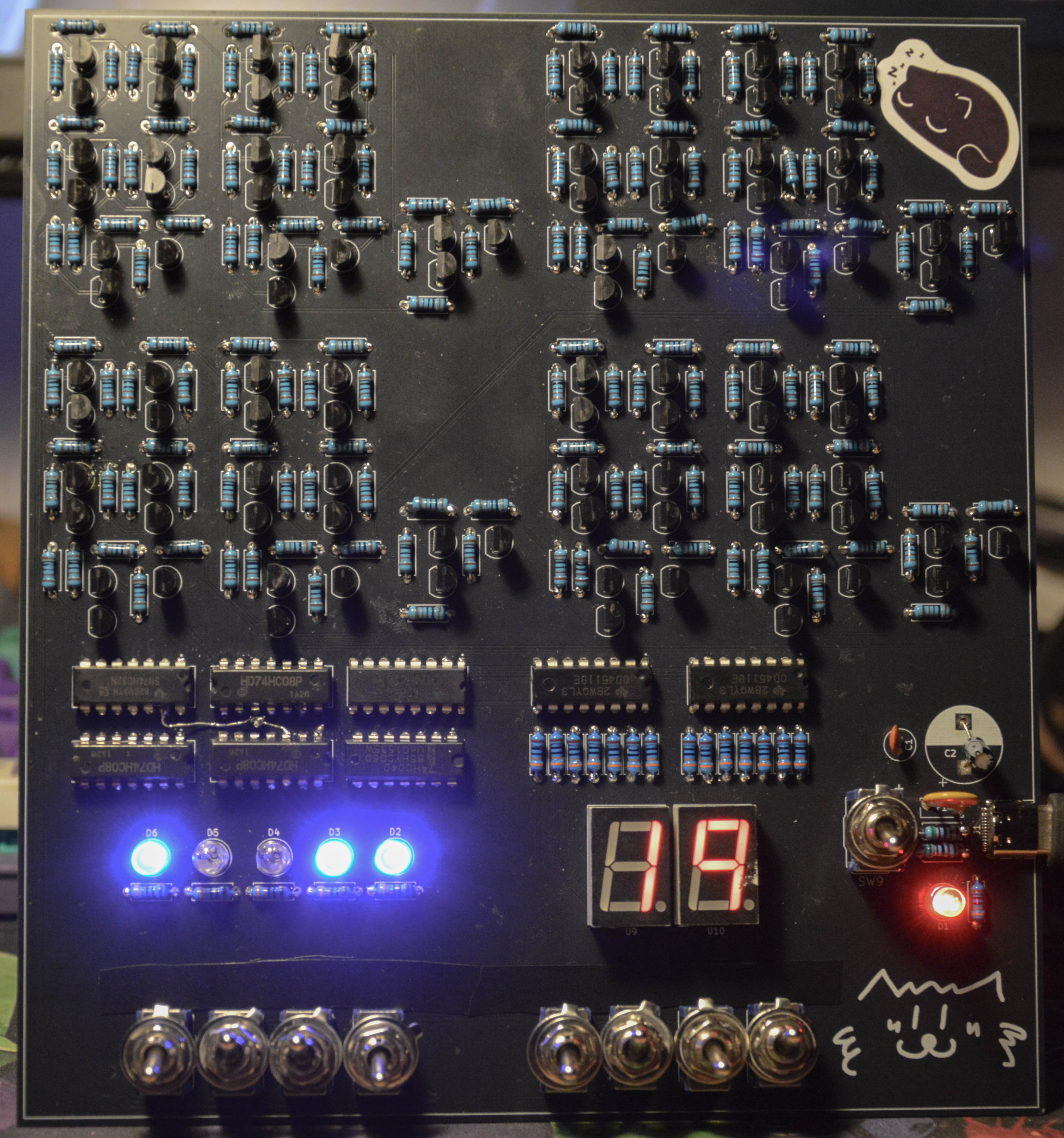
10101₂ = 21₁₀The two displays therefore show:
21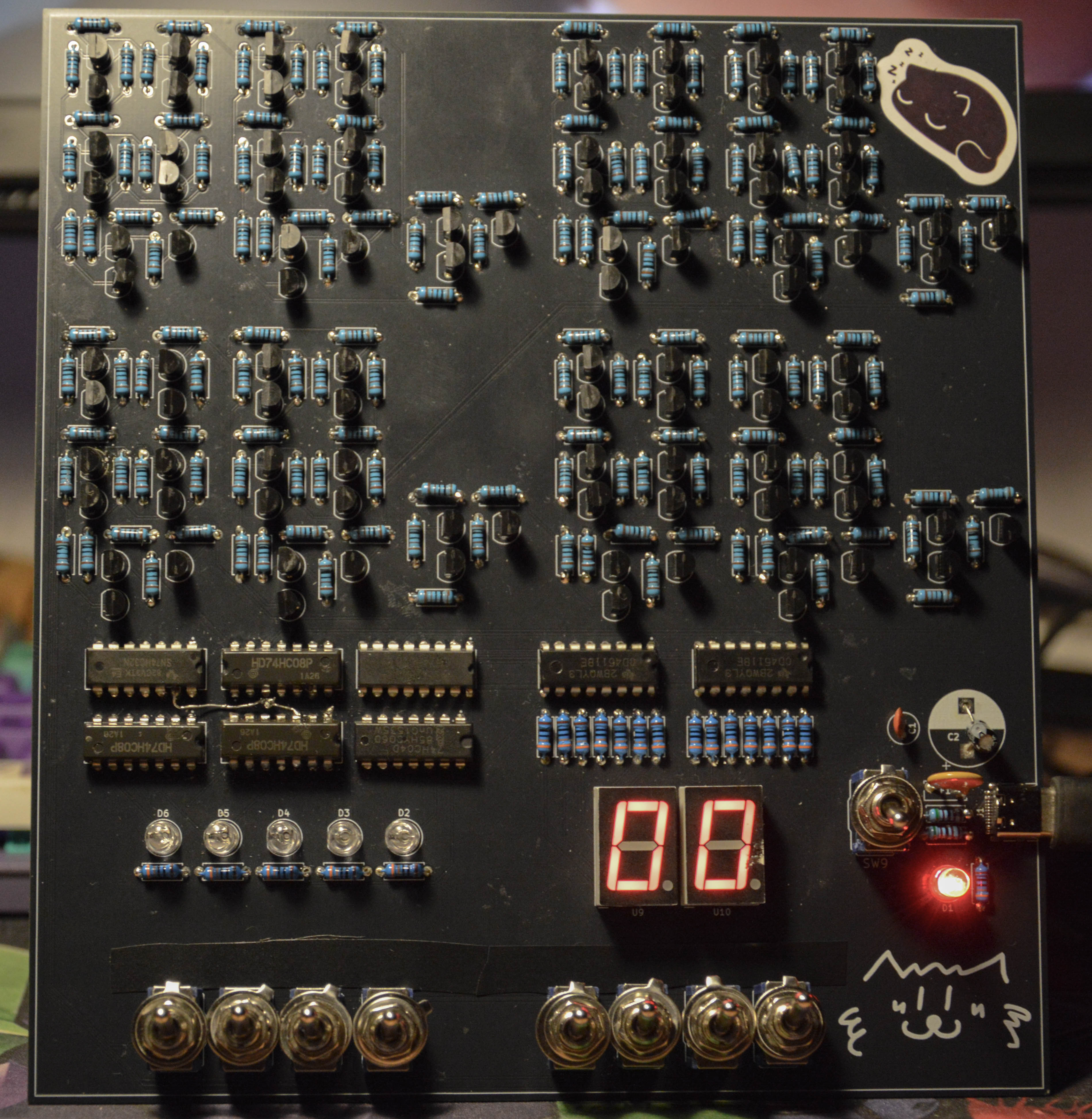
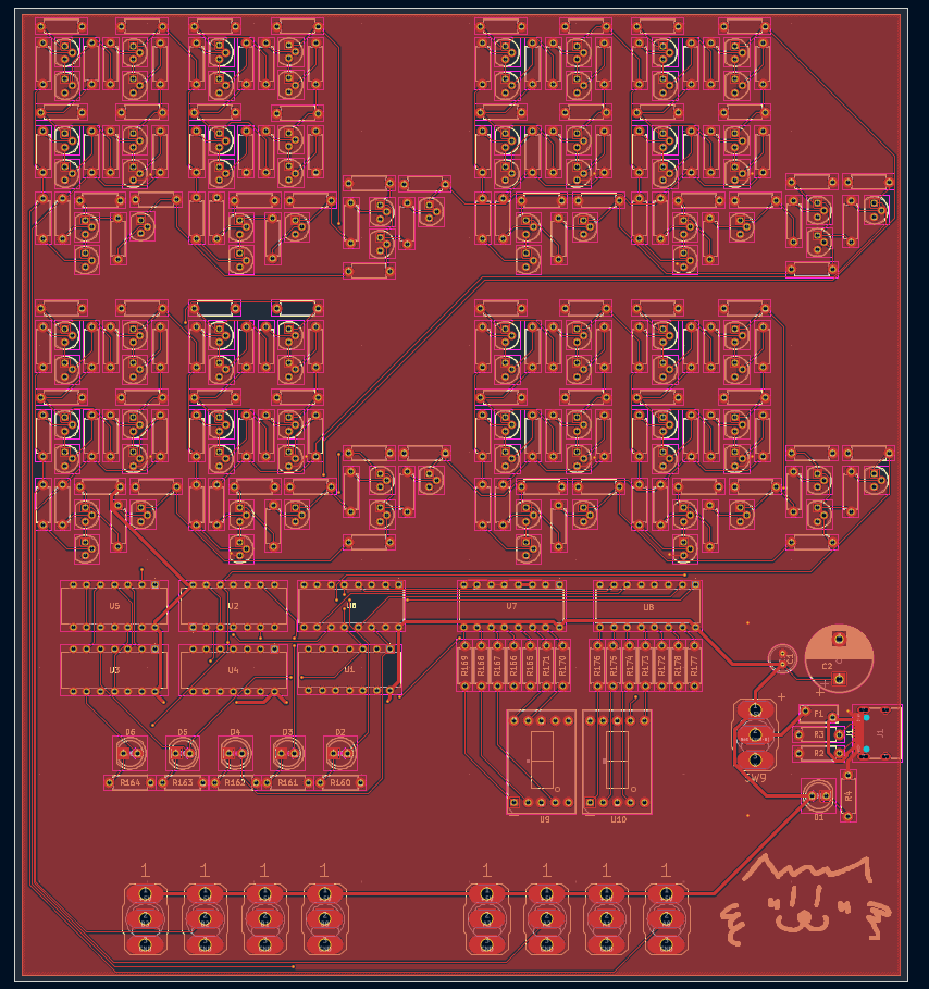
The PCB was designed in KiCad as a two-layer board.
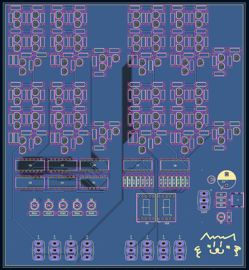
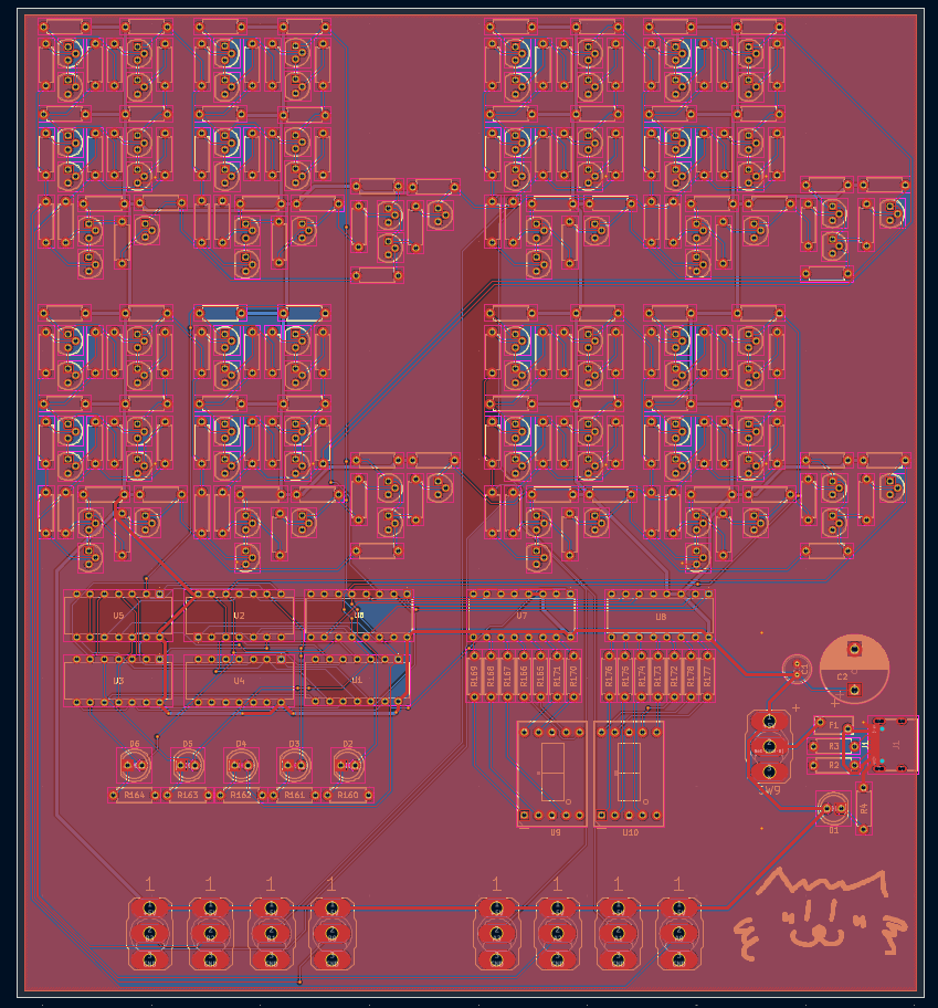
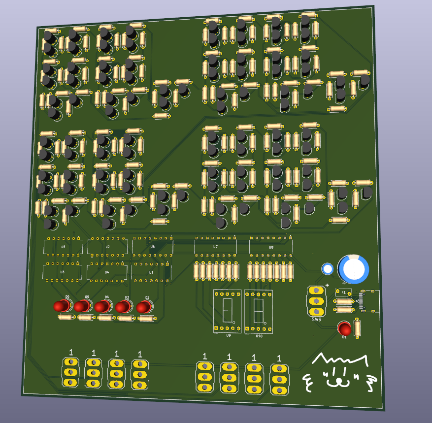
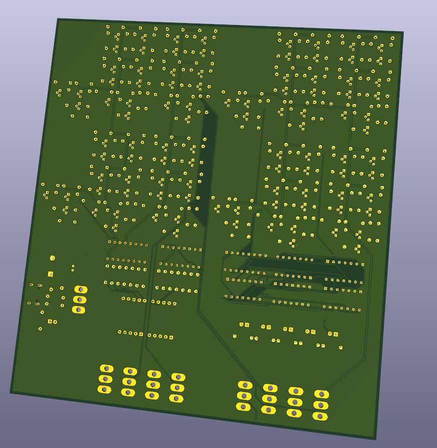
The complete schematic was designed in KiCad and contains the transistor-based adder, logic ICs, BCD conversion, display drivers, inputs, indicators, and power circuitry.
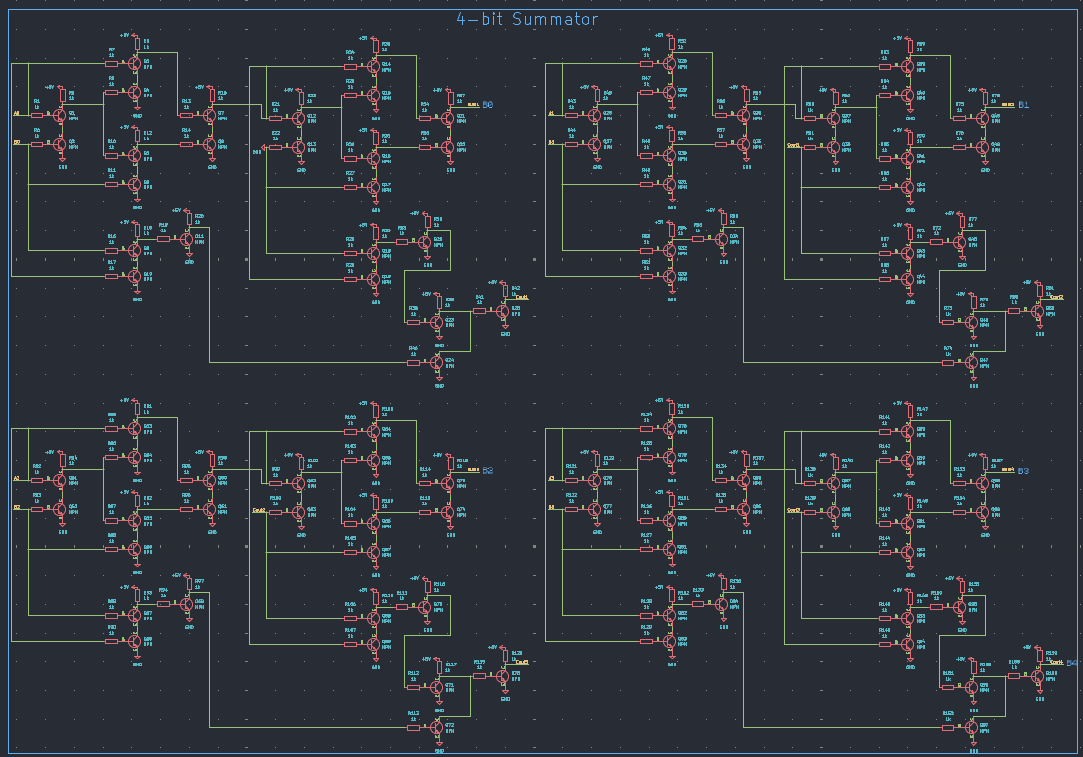
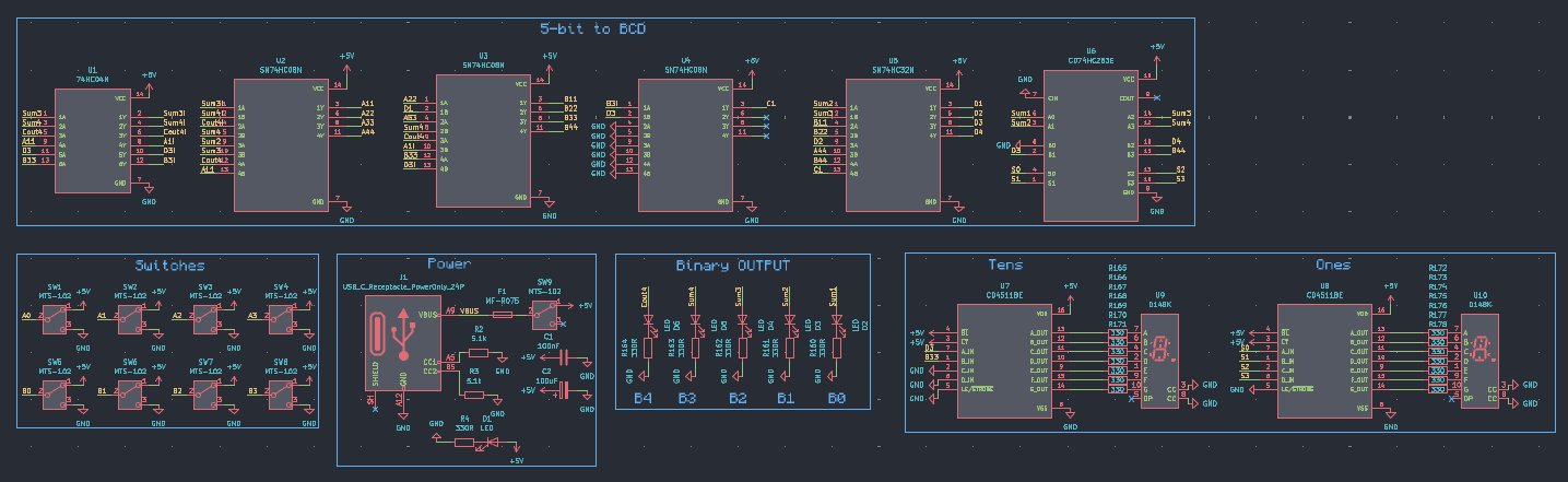 A PDF version of the schematic is included in the
schematic directory.
Open Schematic PDF
An Interactive BOM generated from KiCad is included in the repository. It provides:
Simulation was an important part of the development process. Two different simulation environments were used for different stages of the project.
Falstad was used to learn and develop the transistor-based logic from the ground up. The 4-bit adder was built step by step, starting from transistor-level digital logic and gradually combining the individual stages into a complete working 4-bit adder. A downloadable Falstad simulation file is also included in the repository. Open Simulation Documentation
Tinkercad was used to verify the digital logic and binary-to-BCD conversion. The interactive Tinkercad simulation can be accessed through the simulation documentation.
The project was developed through the following stages:
Concept
   ↓
Logic Design
   ↓
Transistor-Level Development
   ↓
Falstad Simulation
   ↓
Working 4-Bit Adder
   ↓
Tinkercad Simulation
   ↓
KiCad Schematic
   ↓
PCB Layout
   ↓
PCB Manufacturing
   ↓
Component Assembly
   ↓
Hardware Testing
The purpose of this workflow was to validate the logic progressively before moving to the final physical implementation.
The repository contains the files required to reproduce the PCB.
The pcb directory includes:
4-Bit-Transistor-Adder/
│
├── 📁 bom/
│   └── Interactive BOM
│
├── 📁 images/
│   ├── Project photos
│   ├── PCB renders
│   ├── PCB layers
│   ├── Schematic images
│   └── Simulation screenshots
│
├── 📁 pcb/
│   ├── KiCad PCB files
│   └── Gerber files
│
├── 📁 schematic/
│   ├── KiCad schematic
│   └── Schematic PDF
│
├── 📁 simulation/
│   ├── README.md
│   └── Falstad simulation file
│
└── README.md| Qty | Value | Footprint | References |
|---|---|---|---|
| 156 | 1k | Resistor_THT:R_Axial_DIN0207_L6.3mm_D2.5mm_P7.62mm_Horizontal | R1, R10, R11, R100, R101, R102, R103, R104, R105, R106, R107, R108, R109, R110, R111, R112 +140 |
| 100 | NPN | Package_TO_SOT_THT:TO-92 | Q1, Q2, Q10, Q11, Q12, Q13, Q14, Q15, Q16, Q17, Q18, Q19, Q20, Q21, Q22, Q100 +84 |
| 14 | 330 | Resistor_THT:R_Axial_DIN0207_L6.3mm_D2.5mm_P7.62mm_Horizontal | R165, R166, R167, R168, R169, R170, R171, R172, R173, R174, R175, R176, R177, R178 |
| 9 | MTS-102 | MTS-102:MTS-102 | SW1, SW2, SW3, SW4, SW5, SW6, SW7, SW8, SW9 |
| 6 | 330R | Resistor_THT:R_Axial_DIN0207_L6.3mm_D2.5mm_P7.62mm_Horizontal | R4, R160, R161, R162, R163, R164 |
| 6 | LED | LED_THT:LED_D5.0mm | D1, D2, D3, D4, D5, D6 |
| 3 | SN74HC08N | SN74HC08N:DIP794W45P254L1969H508Q14 | U2, U3, U4 |
| 2 | 5.1k | Resistor_THT:R_Axial_DIN0207_L6.3mm_D2.5mm_P7.62mm_Horizontal | R2, R3 |
| 2 | CD4511BE | CD4511BE:DIP794W45P254L1969H508Q16 | U7, U8 |
| 2 | D148K | Display_7Segment:D1X8K | U9, U10 |
| 1 | 100nF | Capacitor_THT:C_Radial_D5.0mm_H5.0mm_P2.00mm | C1 |
| 1 | 100uF | Capacitor_THT:CP_Radial_D12.5mm_P7.50mm | C2 |
| 1 | 74HC04N | 74HC04N:DIP764W47P254L1920H431Q14 | U1 |
| 1 | CD74HC283E | CD74HC283E:DIP794W45P254L1969H508Q16 | U6 |
| 1 | LOGO | footprints:logocat | g |
| 1 | MF-R075 | Fuse:Fuse_Bourns_MF-RHT070 | F1 |
| 1 | SN74HC32N | SN74HC32N:DIP794W45P254L1969H508Q14 | U5 |
| 1 | USB_C_Receptacle_PowerOnly_24P | Connector_USB:USB_C_Receptacle_HRO_TYPE-C-31-M-12 | J1 |


JuanPoueriet/automatic-spork
Máquina de ruleta física de casino. 6 PCBs: pic32main (cerebro), wheel (rueda de LEDs), displaysa/b/c (paneles de 7 segmentos en cascada) y buttons (botonera).

trfaa001/Potentiometer-pedals-to-USB
Arduino project that uses potentiometers as game pedals.

RWeick/REF1011-Sega-GameGear-Pro-Action-Replay
The JEDEC PAL dump, ROM dump, and Kicad PCB files for the Sega GameGear Pro Action Replay.

adham404/Open8-VGA
An 8-bit computer from 74HC logic: microcoded CPU, VGA, PS/2, on-board editor and assembler. Play it in your browser.
It measures 166.4 × 181.6 mm and has 2 copper layers, 1.6 mm thick.
308 parts, built around the CD4511BE, SN74HC08N, 74HC04N and CD74HC283E. The full list of its parts is on this page, with links to each part's symbol and footprint where PCBKit's library has them.
From the PhdWizards/4-Bit-Discrete-Transistor-Adder repository on GitHub, at the commit this page was made from: the board is pcb/Calculator_ver1.kicad_pcb and its schematic schematic/Calculator_ver1.kicad_sch. PCBKit opens the board in the browser, with nothing to install.
Its repository states no licence, so its author keeps all rights: ask PhdWizards before reusing the design.