

2 layers36 × 72 mm
HCP Bridge
JonasE99/HCP-Bridge
🚧 WIP – not yet manufactured or tested. KiCad PCB (one per door) connecting Hörmann series 4 garage door operators (ProMatic/SupraMatic, BUS/RJ12) to Loxone via ESP32-S3 and Wi-Fi.
53 parts1

DIY TEM cell design for EMC measurements
Lisn is an open-source printed circuit board by PetteriAimonen, from the PetteriAimonen/tem-cell repository on GitHub, published under the CC-BY-4.0 licence. It is a 2-layer board of 50 × 49 mm with 36 parts on 18 nets, routed with 139 tracks and 0 vias.
It is built around the DSS16 and BAT54GW. Its parts include 11 resistors, 7 connectors, 6 diodes, 5 capacitors and 4 inductors.
This repository contains FreeCAD and KiCad design files for a TEM cell with integrated LISN.
When combined with a spectrum analyzer, it can be used for EMC pretest measurements.
More construction details are available in my blog article.
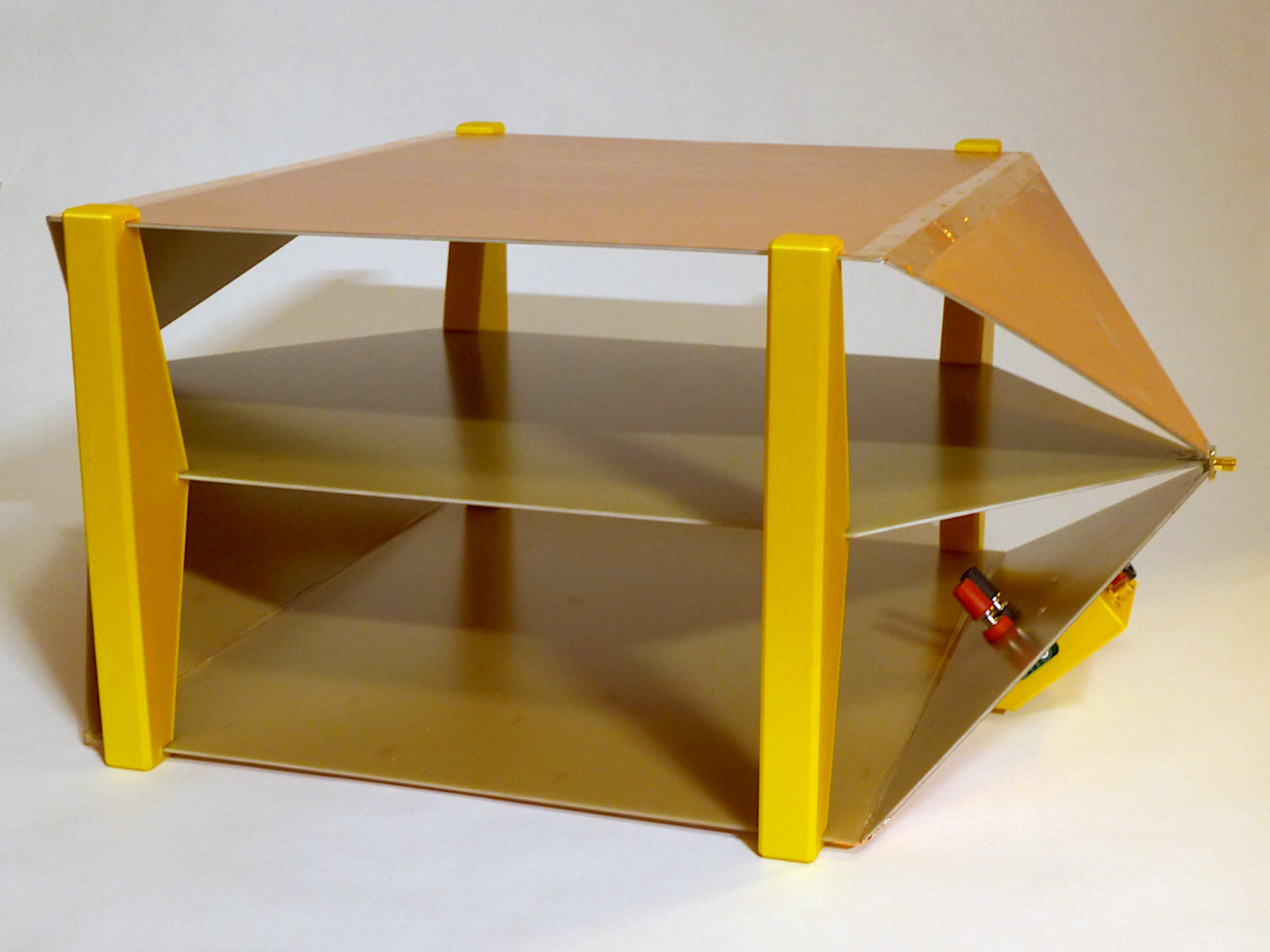
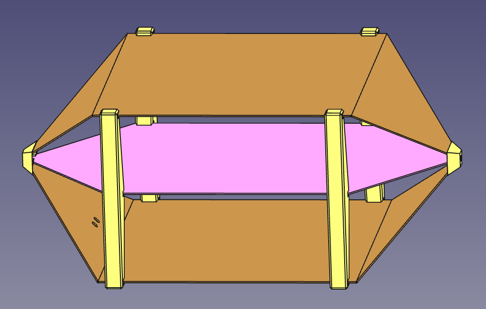
The TEM cell consists of three conductive layers: shield on the top and bottom, and septum in the middle. The width and spacing of the conductors determines the characteristic impedance of the transmission line. The default dimensions are designed for an impedance of 50 ohms, matching most measurement equipment.
Any non-magnetic metal can be used for the construction. The default thickness of 1.6 mm is set for commonly available PCB material.
Coaxial connectors are mounted at each end of the cell. In normal operation one end is terminated with a 50 ohm resistor and the other end is connected to spectrum analyzer or signal generator.
The classic source for custom TEM cell builds is Do-it-Yourself Fabrication of an Open TEM Cell for EMC Pre-compliance by Sandeep M. Satav et al, 2008. It provides the formula for characteristic impedance Z0 of the cell. Goal is to select dimensions so that Z0 equals 50 ohms, to facilitate connection to measurement instruments.
$$ Z_0 = \frac{94.15 \Omega}{\sqrt{\epsilon_r} \cdot \left[ \frac{w}{2d(1 - \frac{t}{2d})} + \frac{C_f}{0.0885 \cdot \epsilon_r} \right] } $$
For air as insulator (εr = 1) and thin material (t → 0), this can be simplified to:
$$ Z_0 = \frac{94.15 \Omega}{\frac{w}{2d} + \frac{C_f}{0.0885}} $$
with the parameters:
The paper further provides value 0.053 pF/cm for the fringe capacitance, based on earlier paper Generation of Standard EM Fields Using TEM Transmission Cells by Myron L. Crawford, 1974. However Satav's paper describes an open TEM cell (with two walls), while Crawford's paper describes a closed TEM cell (with four walls).
Open TEM cell dimensions calculated based on Cf = 0.053 result in a characteristic impedance 1.7 times higher than expected. Using scale models, I have determined that Cf = 0.03 is closer to the correct value for open TEM cells. Relative width of shields and septum affects this value and also uniformity of the electromagnetic field, but optimal configuration is yet unknown.
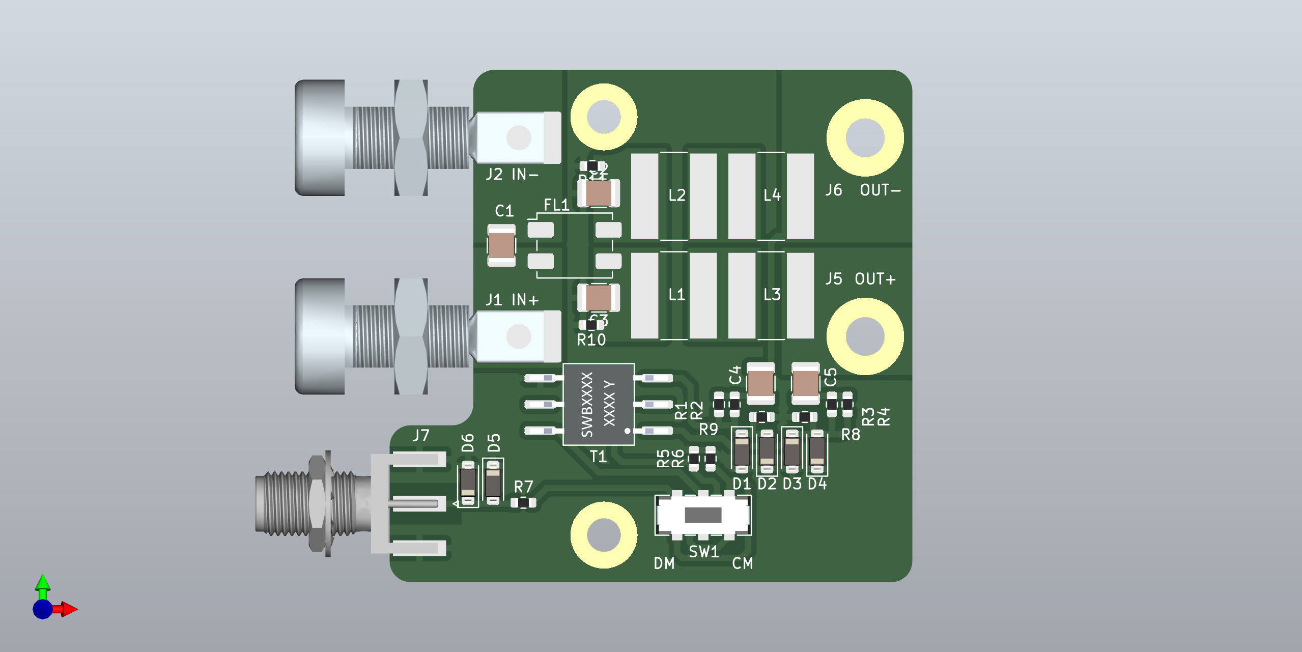
Optionally a LISN can be mounted on the outside of the TEM cell. This is useful for providing a filtered power supply to the device being tested and for measuring conducted emissions.
The LISN is a nominally 50 µH design loosely following CISPR 16 standard, providing 50 ohm impedance to DUT. It is suitable for pretesting use for DC-supplied devices with most EMC standards.
The LISN includes integrated DC block and clamping diodes to limit output to ±0.4 Vpk. Attenuation at the output port is 10 dB. A slide switch selects between common mode and differential mode measurement.
The LISN maximum current is determined by inductor selection and maximum voltage by capacitor ratings. With the listed parts, maximum output current is 1.5 A and voltage 100 VDC.
Correct distance between TEM cell shields and septum is maintained by side support blocks. These should be printed at a low infill ration (5% recommended) to reduce their effect on the dielectric constant.
LISN enclosure is designed to mount on the tapered section. Two binding posts go through the shield to provide a connection on the inside of the cell. Banana jacks and SMA connector are used for connecting a power supply and spectrum analyzer.
The design in OpenTEMCell.FCStd is a FreeCAD parametric design file.
The critical dimensions can be modified in spreadsheet form and the 3D model will update to match.
One possible design is provided as generated files in subdirectory Model_L500mm_W350mm_H200mm.
Wide variety of materials can be used for the construction. I have listed below the materials I have used to construct the Model_L500mm_W350mm_H200mm version:
TEM cell:
| Item | Count |
|---|---|
| FR4 PCB material, one sided, 610x457mm | 3 pcs |
| Square flange SMA connector | 2 pcs |
| SMA terminator | 1 pcs |
LISN:
| Item | Count |
|---|---|
| Binding posts CL1572 (red) and CL1575 (black) | 2 pcs total |
| Banana connectors 108-0902-001 (red) and 108-0903-001 (black) | 2 pcs total |
| SMA connector, edge mount | 1 pcs |
| 9 mm long M3 standoffs | 2 pcs |
| 5 mm long M3 standoffs | 2 pcs |
| M3 countersunk screws | 2 pcs |
| Parts listed in PCB BOM |
Spreadsheet is provided for calculating correction factor for converting TEM cell measurements in dBµV to far field measurements in dBµV/m. The correction factor depends on frequency.
The values are used in place of antenna factor: they simply added to the dBµV reading of the spectrum analyzer at each frequency. The calculation is based on formula:
$$ 20 \cdot \log_{10}\left[ \frac{η_0 \cdot h}{Z_0 \cdot λ \cdot r} \right] $$
with the parameters:
The formula is based on Antenna Gain-Factor Equivalent for TEM Cells by Perry F. Wilson, 2004. Ideal isotropic antenna factor is used as the equivalent far field measurement antenna for converting into field strength units.
NOTE: This application of the formula is my own interpretation of the source material. It may be entirely incorrect. In any case, significant uncertainty remains because DUT geometry affects how effectively fields couple into TEM cell vs. into far field radiation.
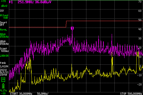
Preset configuration file is provided for TinySA Ultra to simplify measurements.
When applied, the preset configures green trace as correction factor table and subtracts it from the measurement traces. Output readings will approximate dBµV/m. Yellow trace is live measurement and purple trace is maximum level hold. Red trace is example of typical radiated emission limits, actual values will depend on applicable standard.
The spectrum analyzer settings used do not match any of the established EMC standards. To achieve high scanning speed, a large resolution bandwidth and small dwell time of about 0.2 ms is used. The detector is closest to average measurement type, though the maximum hold will retain the peak value if it hits the dwell time window. These limitations will result in significant inaccuracies when measuring narrow-band or pulsed emissions.
Signal coupling in TEM cell will depend both on the magnetic and electric field orientations. One technique is to rotate the DUT into different orientations and let the maximum hold capture the largest emissions. At the end, power down DUT so that you can compare background noise against any spikes from the device.
All the design materials are available under CC-BY-4.0 license. Preferred attribution:
© 2023 Petteri Aimonen. Licensed under CC-BY-4.0. https://essentialscrap.com/
| Qty | Value | Footprint | References |
|---|---|---|---|
| 5 | 1µF | Capacitor_SMD:C_1210_3225Metric | C1, C2, C3, C4, C5 |
| 4 | 22µH | Inductor_SMD:L_Bourns-SRN8040_8x8.15mm | L1, L2, L3, L4 |
| 4 | 50 | Resistor_SMD:R_0603_1608Metric | R1, R2, R3, R4 |
| 4 | DSS16 | Diode_SMD:D_SOD-123 | D1, D2, D3, D4 |
| 2 | 100k | Resistor_SMD:R_0603_1608Metric | R10, R11 |
| 2 | 68 | Resistor_SMD:R_0603_1608Metric | R8, R9 |
| 2 | 82 | Resistor_SMD:R_0603_1608Metric | R5, R6 |
| 2 | BAT54GW | Diode_SMD:D_SOD-123 | D5, D6 |
| 2 | GND | MountingHole:MountingHole_3.2mm_M3_Pad | J3, J4 |
| 1 | 30 | Resistor_SMD:R_0603_1608Metric | R7 |
| 1 | CM7060 | Inductor_SMD:L_CommonModeChoke_TDK_ACM7060 | FL1 |
| 1 | DPDT | footprints:SW_DPDT_CK_JS202011JCQN | SW1 |
| 1 | IN+ | footprints:BANANA_JACK_108-0902-001 | J1 |
| 1 | IN- | footprints:BANANA_JACK_108-0902-001 | J2 |
| 1 | OUT+ | MountingHole:MountingHole_3.7mm_Pad | J5 |
| 1 | OUT- | MountingHole:MountingHole_3.7mm_Pad | J6 |
| 1 | SMA | Connector_Coaxial:SMA_Amphenol_132289_EdgeMount | J7 |
| 1 | SWB2010 | footprints:SWB2010-SMLD | T1 |
JonasE99/HCP-Bridge
🚧 WIP – not yet manufactured or tested. KiCad PCB (one per door) connecting Hörmann series 4 garage door operators (ProMatic/SupraMatic, BUS/RJ12) to Loxone via ESP32-S3 and Wi-Fi.

gustebeast/public-steel-guitar
A pedal steel guitar you can build yourself, from parts anyone can buy.

EwoudVV/arpeggiator
12-note analog arpeggiator with a 1/2/3 octave range, custom pcb and printed case


hoglet67/RGBtoHDMI
Bare-metal Raspberry Pi project that provides pixel-perfect sampling of Retro Computer RGB/YUV video and conversion to HDMI

hackclub/OnBoard
💡 Join 1,000 teenagers and make your first PCB with a $100 grant!

It measures 50 × 49 mm and has 2 copper layers, 1.6 mm thick.
36 parts, built around the DSS16 and BAT54GW. The full list of its parts is on this page, with links to each part's symbol and footprint where PCBKit's library has them.
From the PetteriAimonen/tem-cell repository on GitHub, at the commit this page was made from: the board is lisn/lisn.kicad_pcb and its schematic lisn/lisn.kicad_sch. PCBKit opens the board in the browser, with nothing to install.
Its repository publishes it under the CC-BY-4.0 licence: you may reuse it on that licence's terms (keep the author's notice, and for a copyleft licence share your changes alike).