
2 layers34 × 18 mm

 perriestudios/cse475-pcb-tutorial
This repo contains the design files modified for the Embedded Systems Capstone class taught at University of Washington during Autumn'22.
Cse475-pcb tutorial is an open-source printed circuit board by perriestudios, from the perriestudios/cse475-pcb-tutorial repository on GitHub. It is a 2-layer board of 18.3 × 34.5 mm with 17 parts on 18 nets, routed with 91 tracks and 12 vias.
It is built around the ATSAMD10C14A-SSN. Its parts include 4 resistors, 4 connectors, 3 capacitors, 2 ICs and 2 diodes. It belongs with the SAM D and SAM boards of this library.
[CSE/EE 475] PCB Tutorial
This repository contains all the files used for the PCB tutorial I taught in the Embedded Systems Capstone class. The base design was derived from the work of Mike's(MalphasWats) hawk project. Hawk is well documented and highlights most concepts of PCB Design required for this class.
I made the following changes to the design to ensure a few other useful concepts were also covered:
The schematic with the changes looks like this:
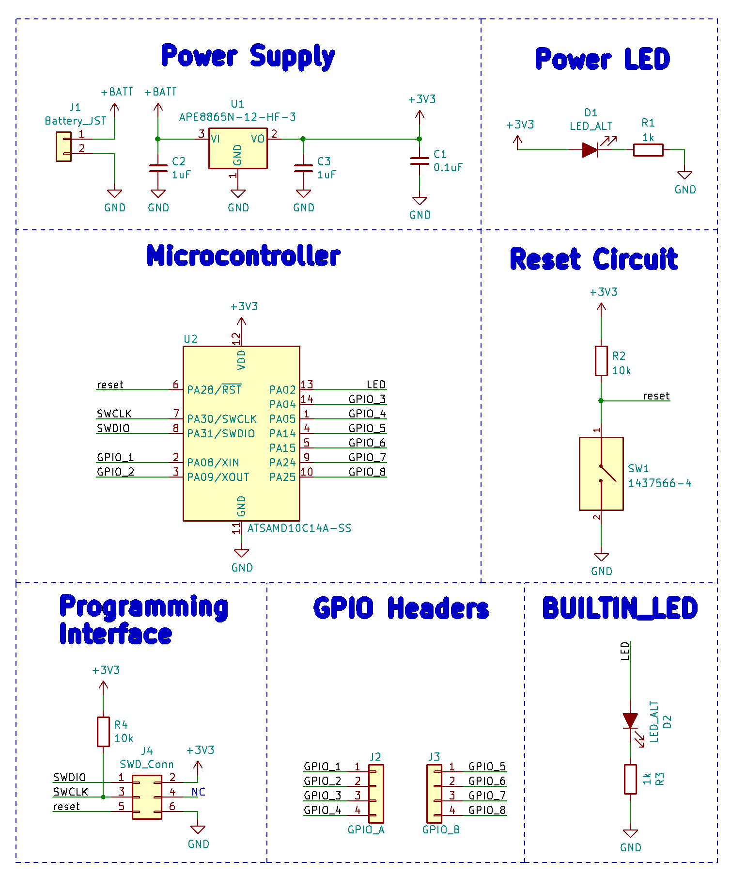
Here's how the completed PCB looks like:
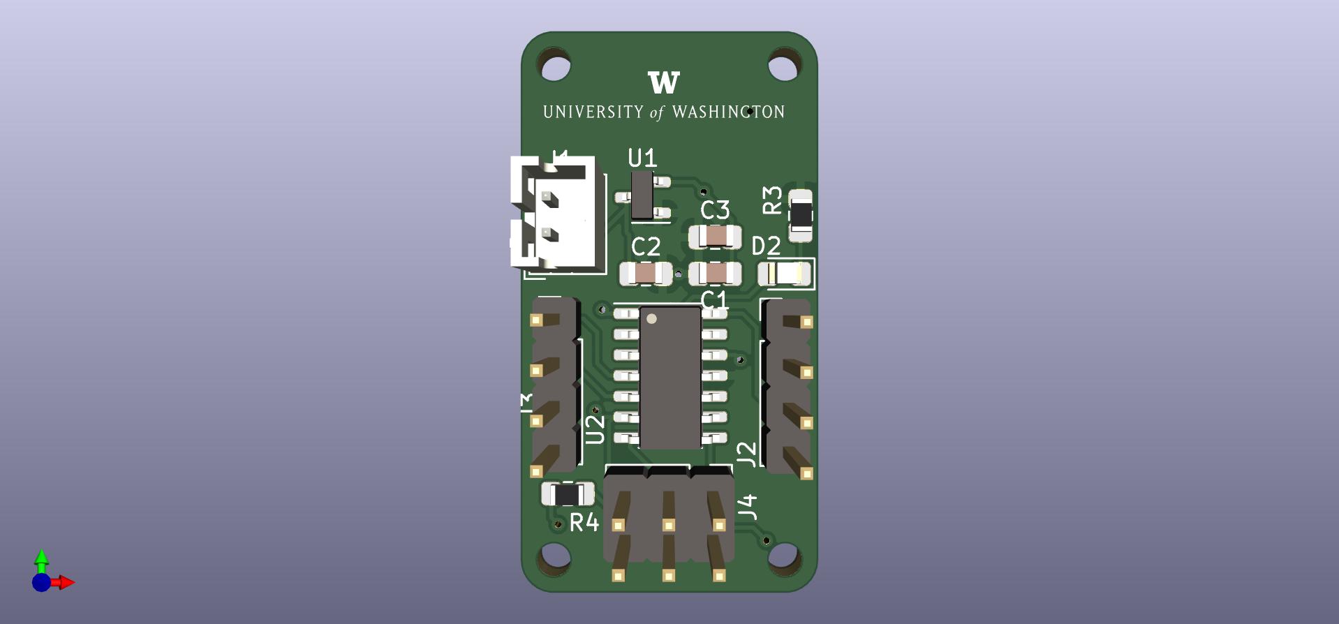
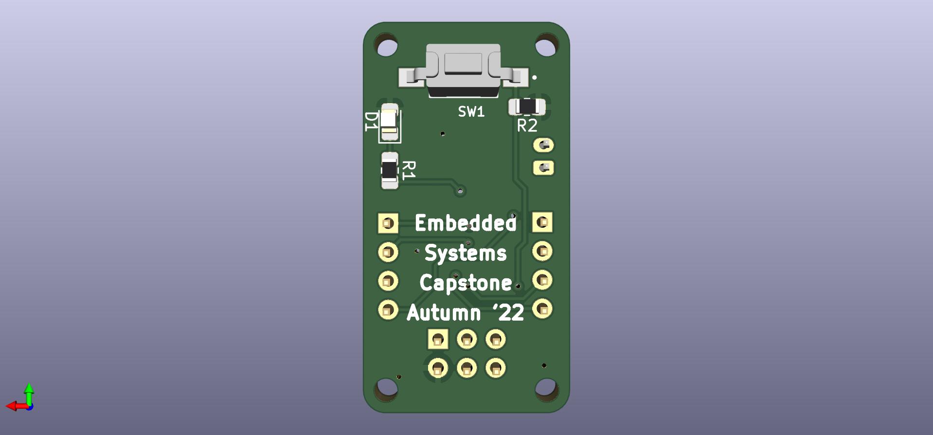
The slides used for the presentation can be found here and the dxf file imported into the design can be found here
| Qty | Value | Footprint | References |
|---|---|---|---|
| 2 | 1uF | Capacitor_SMD:C_0805_2012Metric_Pad1.15x1.40mm_HandSolder | C2, C3 |
| 2 | LED_ALT | LED_SMD:LED_0805_2012Metric_Pad1.15x1.40mm_HandSolder | D1, D2 |
| 1 | 0.1uF | Capacitor_SMD:C_0805_2012Metric_Pad1.15x1.40mm_HandSolder | C1 |
| 1 | 10k | Resistor_SMD:R_0805_2012Metric_Pad1.20x1.40mm_HandSolder | R2 |
| 1 | 10k | Resistor_SMD:R_0805_2012Metric_Pad1.15x1.40mm_HandSolder | R4 |
| 1 | 1437566-4 | Custom:SW_1437566-4 | SW1 |
| 1 | 1k | Resistor_SMD:R_0805_2012Metric_Pad1.20x1.40mm_HandSolder | R1 |
| 1 | 1k | Resistor_SMD:R_0805_2012Metric_Pad1.15x1.40mm_HandSolder | R3 |
| 1 | APE8865N-12-HF-3 | Package_TO_SOT_SMD:SOT-23 | U1 |
| 1 | ATSAMD10C14A-SS | Package_SO:SOIC-14_3.9x8.7mm_P1.27mm | U2 |
| 1 | Battery_JST | Connector_JST:JST_PH_B2B-PH-K_1x02_P2.00mm_Vertical | J1 |
| 1 | GPIO_A | Connector_PinHeader_2.54mm:PinHeader_1x04_P2.54mm_Vertical | J2 |
| 1 | GPIO_B | Connector_PinHeader_2.54mm:PinHeader_1x04_P2.54mm_Vertical | J3 |
| 1 | LOGO | LOGO | G*** |
| 1 | SWD_Conn | Connector_PinHeader_2.54mm:PinHeader_2x03_P2.54mm_Vertical | J4 |
It measures 18.3 × 34.5 mm and has 2 copper layers, 1.6 mm thick.
17 parts, built around the ATSAMD10C14A-SSN. The full list of its parts is on this page, with links to each part's symbol and footprint where PCBKit's library has them.
From the perriestudios/cse475-pcb-tutorial repository on GitHub, at the commit this page was made from: the board is cse475-pcb-tutorial.kicad_pcb and its schematic cse475-pcb-tutorial.kicad_sch. PCBKit opens the board in the browser, with nothing to install.
Its repository states no licence, so its author keeps all rights: ask perriestudios before reusing the design.


hoglet67/RGBtoHDMI
Bare-metal Raspberry Pi project that provides pixel-perfect sampling of Retro Computer RGB/YUV video and conversion to HDMI


hackclub/OnBoard
💡 Join 1,000 teenagers and make your first PCB with a $100 grant!

DDeGonge/OS-ARM
This arm is not industrial and it will not be fast, but that is not my goal. But it will hopefully be a very nice looking arm fully capable of 6dof motion, cheap enough to keep it accessable but capable enough to…
