2 layers105.4 × 215.6 mm
MIDI Sax
hackclub/OnBoard
💡 Join 1,000 teenagers and make your first PCB with a $100 grant!
75 parts915
 peej/for-split-keyboard32
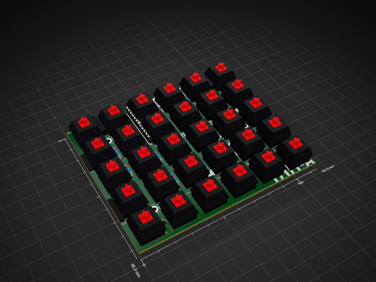
Split Infinitive, a 6x5x2 ortholinear split keyboard PCB
For split is an open-source printed circuit board by peej, from the peej/for-split-keyboard repository on GitHub, published under the MIT licence. It is a 2-layer board of 114.3 × 95.3 mm with 75 parts on 55 nets, routed with 932 tracks and 43 vias.
Its parts include 30 diodes, 2 connectors and 1 IC. It belongs with the keyboards and input boards and the AVR (ATmega, ATtiny) boards of this library.
Split Infinitive is a 6x5x2 key ortholinear split keyboard PCB.
The goal of this project is to build a Let's Split keyboard clone with a number of alternative features:
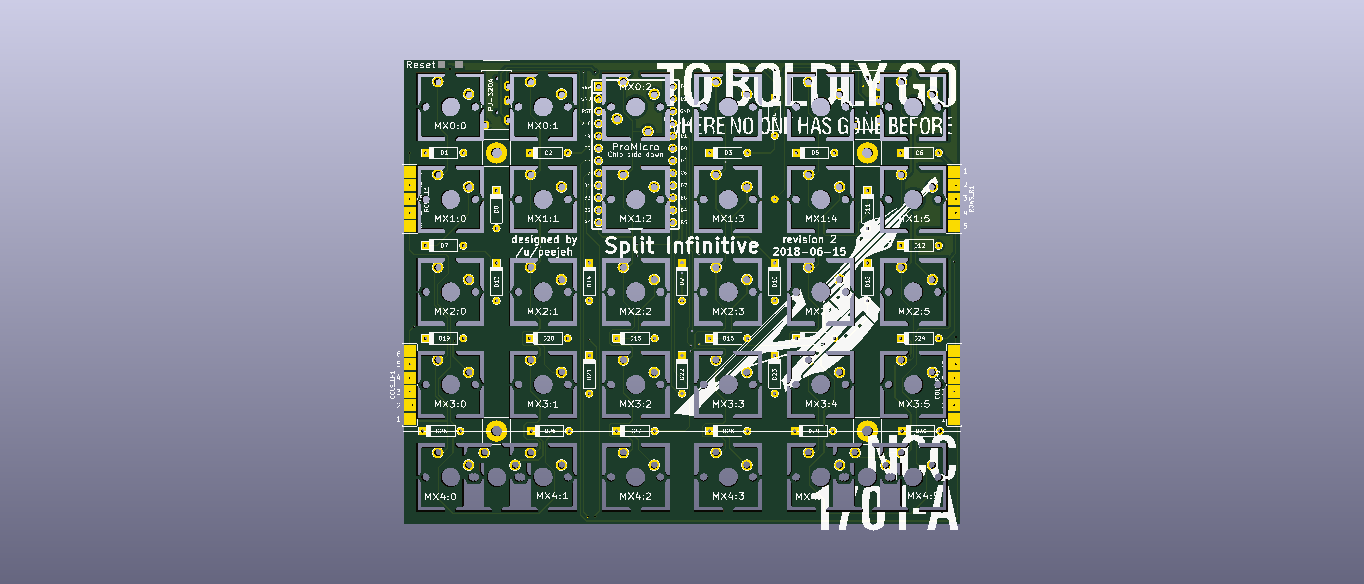
PCBs can be manufactuered by a variety of online PCB fabricators, the PCB is 114x95mm. You can use PCBShopper to search for the best price.
The zip file in the gerber directory contains the gerber files your fabricator will need to make the PCB for-split.zip PCB.
When uploading the gerber zip files, use the default PCB settings. The plate PCB thickness should be 1.6mm for the switches to snap into the plate securely.
| Qty | Value | Footprint | References |
|---|---|---|---|
| 30 | DIODE | idle-hands:DIODE | D1, D2, D10, D11, D12, D13, D14, D15, D16, D17, D18, D19, D20, D21, D22, D23 +14 |
| 4 | MountingHole | Mounting_Holes:MountingHole_2.2mm_M2_Pad | Hole, Hole, Hole, Hole |
| 2 | Conn_01x05 | idle-hands:CONNECTOR_5 | ROWS_L1, ROWS_R1 |
| 2 | Conn_01x06 | idle-hands:CONNECTOR_6 | COLS_LH1, COLS_RH1 |
| 2 | TRRS | idle-hands:PJ-320A | J1, J2 |
| 1 | ExtraData | idle-hands:Square_Pad | EXTRADATA1 |
| 1 | Ground | idle-hands:Single_Pad | GROUND1 |
| 1 | LOGO | idle-hands:boldy1 | G*** |
| 1 | MX0:10 | idle-hands:MX_CUTOUT | MX0:1 |
| 1 | MX0:11 | idle-hands:MX_CUTOUT | MX0:0 |
| 1 | MX0:6 | idle-hands:MX_CUTOUT | MX0:5 |
| 1 | MX0:7 | idle-hands:MX_CUTOUT | MX0:4 |
| 1 | MX0:8 | idle-hands:MX_CUTOUT | MX0:3 |
| 1 | MX0:9 | idle-hands:MX_CUTOUT_NTHSTH | MX0:2 |
| 1 | MX1:10 | idle-hands:MX_CUTOUT | MX1:1 |
| 1 | MX1:11 | idle-hands:MX_CUTOUT | MX1:0 |
| 1 | MX1:6 | idle-hands:MX_CUTOUT | MX1:5 |
| 1 | MX1:7 | idle-hands:MX_CUTOUT | MX1:4 |
| 1 | MX1:8 | idle-hands:MX_CUTOUT | MX1:3 |
| 1 | MX1:9 | idle-hands:MX_CUTOUT | MX1:2 |
| 1 | MX2:10 | idle-hands:MX_CUTOUT | MX2:1 |
| 1 | MX2:11 | idle-hands:MX_CUTOUT | MX2:0 |
| 1 | MX2:6 | idle-hands:MX_CUTOUT | MX2:5 |
| 1 | MX2:7 | idle-hands:MX_CUTOUT | MX2:4 |
| 1 | MX2:8 | idle-hands:MX_CUTOUT | MX2:3 |
| 1 | MX2:9 | idle-hands:MX_CUTOUT | MX2:2 |
| 1 | MX3:10 | idle-hands:MX_CUTOUT | MX3:1 |
| 1 | MX3:11 | idle-hands:MX_CUTOUT | MX3:0 |
| 1 | MX3:6 | idle-hands:MX_CUTOUT | MX3:5 |
| 1 | MX3:7 | idle-hands:MX_CUTOUT | MX3:4 |
| 1 | MX3:8 | idle-hands:MX_CUTOUT | MX3:3 |
| 1 | MX3:9 | idle-hands:MX_CUTOUT | MX3:2 |
| 1 | MX4:10 | idle-hands:MX2U_CUTOUT | MX4:1 |
| 1 | MX4:11 | idle-hands:MX | MX4:0 |
| 1 | MX4:6 | idle-hands:MX2U_CUTOUT | MX4:5 |
| 1 | MX4:7 | idle-hands:MX | MX4:4 |
| 1 | MX4:8 | idle-hands:MX_CUTOUT | MX4:3 |
| 1 | MX4:9 | idle-hands:MX_CUTOUT | MX4:2 |
| 1 | ProMicro | idle-hands:Pro_Micro_ChipSideDown | U1 |
| 1 | Reset | idle-hands:Single_Pad | RESET1 |
It measures 114.3 × 95.3 mm and has 2 copper layers, 1.6 mm thick.
75 parts. The full list of its parts is on this page, with links to each part's symbol and footprint where PCBKit's library has them.
From the peej/for-split-keyboard repository on GitHub, at the commit this page was made from: the board is for-split.kicad_pcb. PCBKit opens the board in the browser, with nothing to install.
Its repository publishes it under the MIT licence: you may reuse it on that licence's terms (keep the author's notice, and for a copyleft licence share your changes alike).
hackclub/OnBoard
💡 Join 1,000 teenagers and make your first PCB with a $100 grant!


JGAguado/Smart_Plant
The Smart Plant is a board that can be plugged directly on the soil, close to the plant, that allows the measurement of the environment (soil moisture, environment temperature & illuminance), and presents the…


StoneRose35/cortexguitarfx
guitar effects processor implemented on various arm cortex platforms


cnlohr/cnhardware
My dumping grounds for all my kicad projects and random hardware bringup.

thebiguno/microcontroller-projects
A home for a bunch of microcontroller projects which don't warrant their own repos.