

2 layers105 × 60 mm
Personal blog
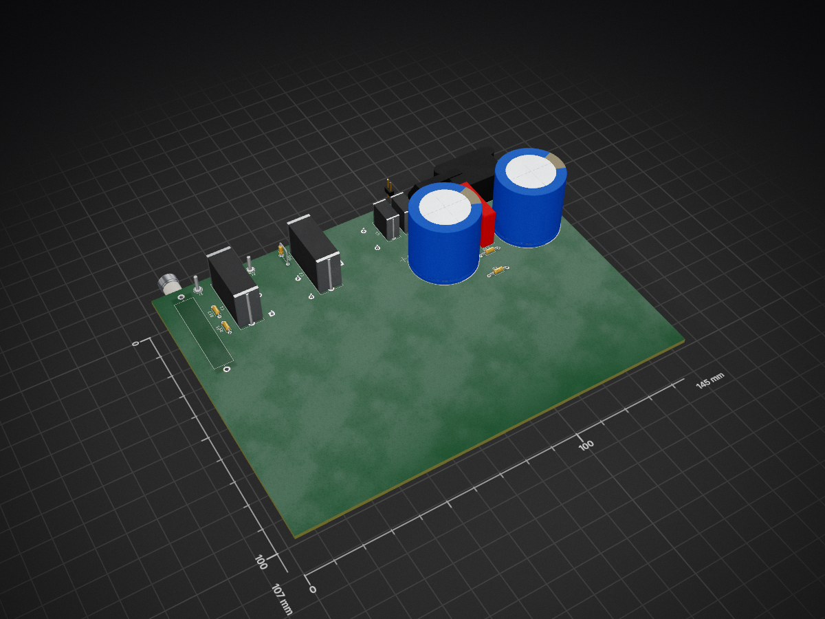
At psu is an open-source printed circuit board by pcbanalyst, from the pcbanalyst/pcbanalyst.github.io repository on GitHub. It is a 2-layer board of 145 × 107 mm with 21 parts on 18 nets.
It is built around the B40R. Its parts include 7 capacitors, 4 resistors, 3 inductors, 2 connectors and 1 switch. It belongs with the power boards of this library.
| Qty | Value | Footprint | References |
|---|---|---|---|
| 2 | C | Capacitor_THT:C_Rect_L11.5mm_W5.0mm_P10.00mm_MKT | C3, C4 |
| 2 | C | Capacitor_THT:C_Rect_L24.0mm_W8.6mm_P22.50mm_MKT | C1, C2 |
| 2 | CP | Capacitor_THT:CP_Radial_D25.0mm_P10.00mm_SnapIn | C6, C7 |
| 2 | Conn_01x01 | Connector_Pin:Pin_D1.3mm_L11.0mm | J1, J2 |
| 2 | L_Coupled | Inductor_THT:Choke_Schaffner_RN112-04-17.7x17.1mm | L1, L2 |
| 2 | R | Resistor_THT:R_Axial_DIN0204_L3.6mm_D1.6mm_P5.08mm_Horizontal | R1, R17 |
| 2 | R | Resistor_THT:R_Axial_DIN0204_L3.6mm_D1.6mm_P7.62mm_Horizontal | R2, R12 |
| 2 | Thermistor | Resistor_THT:R_Axial_DIN0204_L3.6mm_D1.6mm_P5.08mm_Vertical | TH1, TH3 |
| 1 | B40R | Diode_THT:Diode_Bridge_Vishay_GBL | DB1 |
| 1 | C | Capacitor_THT:C_Rect_L19.0mm_W5.0mm_P15.00mm_MKS4 | C12 |
| 1 | Fuse | Fuse:Fuse_SunFuse-6HP | F1 |
| 1 | L_Coupled_Small | Inductor_THT:L_Mount_Lodestone_VTM120 | L3 |
| 1 | SW_SPST | Connector_PinHeader_2.00mm:PinHeader_1x02_P2.00mm_Vertical | SW2 |
It measures 145 × 107 mm and has 2 copper layers, 1.6 mm thick.
21 parts, built around the B40R. The full list of its parts is on this page, with links to each part's symbol and footprint where PCBKit's library has them.
From the pcbanalyst/pcbanalyst.github.io repository on GitHub, at the commit this page was made from: the board is assets/boards/astec/at_psu/kicad/kicad.kicad_pcb and its schematic assets/boards/nintendo/nus-002(eur)/nus-002/nus-002.kicad_sch. PCBKit opens the board in the browser, with nothing to install.
Its repository states no licence, so its author keeps all rights: ask pcbanalyst before reusing the design.


thorsten-l/ESP8266-WiFi-Doorbell-Gateway
A gateway for your doorbell button ;-)


Nayan9ine/Mosquito_Swatter_PCB
Reverse Engineered pcb design of a mosquito swatter circuit built using KiCad

nicolafehr/Umschaltplatine_Mobacom
PCB um die Steuerung einer Testanlage mit verschiedenen Zentralen zu ermöglichen. Zudem können verschiedene Gleisabschnitte angesteuert werden können.


AndmDam/kiCad_repo
Repositorio de mis archivos de mis proyectos de kicad.