
2 layers76.3 × 49.6 mm

 pazambranosauc/esp32-devboard
Two-layer ESP32-WROOM-32 dev board in KiCad: USB-C, CP2102N with auto-reset, AMS1117, breadboard headers. Rev B after a design review of rev A.
Customized ESP-32 is an open-source printed circuit board by pazambranosauc, from the pazambranosauc/esp32-devboard repository on GitHub. It is a 2-layer board of 30 × 64 mm with 28 parts on 62 nets, routed with 544 tracks and 45 vias.
It is built around the ESP32-WROOM-32, AMS1117-3.3 and MMBT3904. Its parts include 9 resistors, 7 capacitors, 3 ICs, 3 connectors and 2 transistors. It belongs with the microcontroller boards boards and the ESP32 boards of this library.


A two-layer ESP32-WROOM-32 development board designed from a blank schematic: USB-C, an AMS1117-3.3 regulator, a CP2102N USB-UART bridge with two-transistor auto-reset, and two breadboard-spaced 20-pin headers. It's sized for hand assembly: 0603 passives, 1206 tantalums, 2.54 mm headers.
Status: Rev B layout complete, not yet fabricated. Rev A was cancelled before production after a design review found three faults (below). Bring-up results will be added here once the boards arrive.
| Top | Bottom |
|---|---|
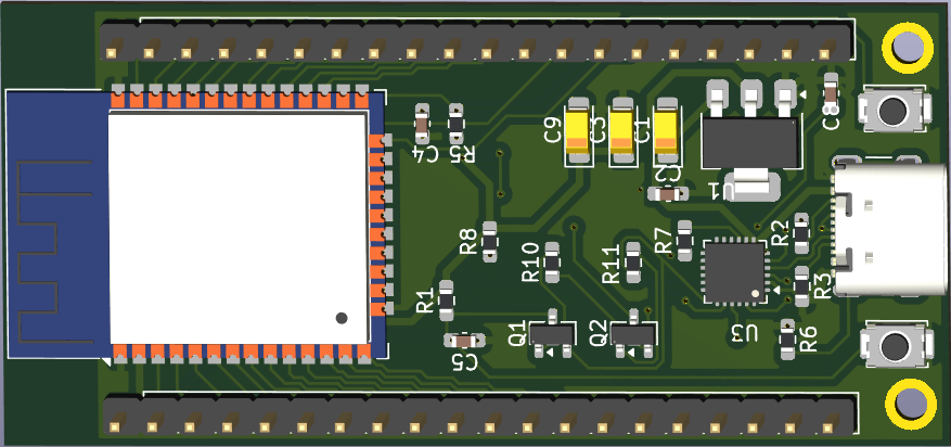 | 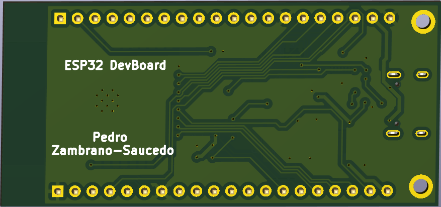 |
| Board | 30.0 × 64.0 mm, 2 layers, GND pour on both layers |
| MCU | ESP32-WROOM-32 (antenna keep-out on every layer, no copper under the antenna) |
| USB | USB-C receptacle (GCT USB4105), USB 2.0, 5.1 kΩ on CC1 and CC2 so it works either way up |
| USB-UART | CP2102N (QFN-24), DTR/RTS auto-reset through two MMBT3904s |
| Power | 5 V USB → AMS1117-3.3, 10 µF tantalum in and out, 100 nF decoupling at each IC |
| I/O | 2 × 20-pin 2.54 mm headers, rows 25.4 mm apart (fits a breadboard) |
| Buttons | EN (reset) and IO0 (boot) |
| Routing | 0.25 mm signals, 0.5 mm power (USB_VBUS, VDD, GND), necked down to 0.2 mm at fine-pitch pins |
USB-C ─┬─ VBUS ──┬─ AMS1117-3.3 ── VDD (3.3 V) ─┬─ ESP32-WROOM-32
       │         └─ CP2102N VREGIN / VBUS        └─ CP2102N VIO, pull-ups, headers
       ├─ D+/D− ─── CP2102N ── TXD/RXD ───────────── ESP32 RXD0/TXD0
       │                    └─ DTR/RTS ─ Q1/Q2 ──── EN / IO0   (auto-reset into bootloader)
       └─ CC1/CC2 ─ 5.1 kΩ each to GND (identifies the board as a USB sink)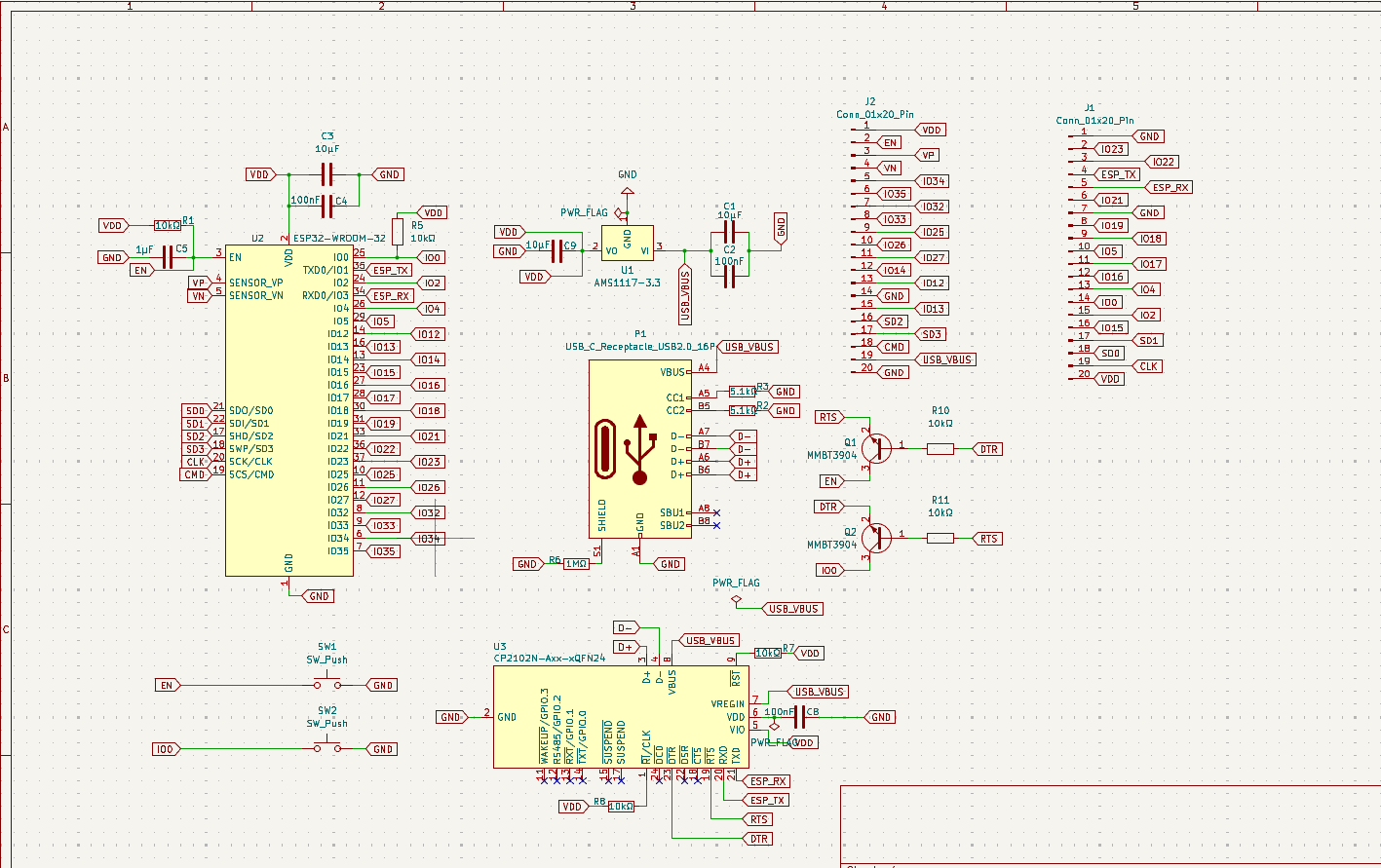
Rev A was laid out and submitted to JLCPCB. A net-by-net review of the board file found three faults, so I cancelled the order before it went into production.
| # | Rev A fault | Why it was missed | Rev B fix |
|---|---|---|---|
| 1 | The 3.3 V regulator had no input. USB 5 V (USB_VBUS) only reached the CP2102N's VREGIN pin. The AMS1117's input was on a separate net (UART_VBUS) tied only to the CP2102N's VBUS sense pin. The input caps were in series instead of to GND. The board would never have powered on. | A PWR_FLAG on the regulator input told ERC the net was powered, which hid the error. | USB 5 V feeds the regulator and both CP2102N VBUS pins, the caps go to GND, and the masking PWR_FLAG is removed. |
| 2 | The reset and boot buttons did nothing. Each switch pulled EN or IO0 to GND through a reverse-biased LED, so the pin never went low. | ERC can't see it: every connection is valid, only the diode direction is wrong. | The switches go directly to EN and IO0, and the LEDs are removed. |
| 3 | Auto-reset was AC-coupled. The transistor bases were driven through 100 nF capacitors instead of resistors, giving only edge pulses where esptool needs IO0 held low while EN rises. | ERC can't see it: the topology is right, only the component type is wrong. | 10 kΩ base resistors (R10, R11). |
Also changed for Rev B:
The original Rev A schematic is kept in hardware/rev-a/, with a screenshot, for comparison.
| Layout, front copper | Layout, back copper |
|---|---|
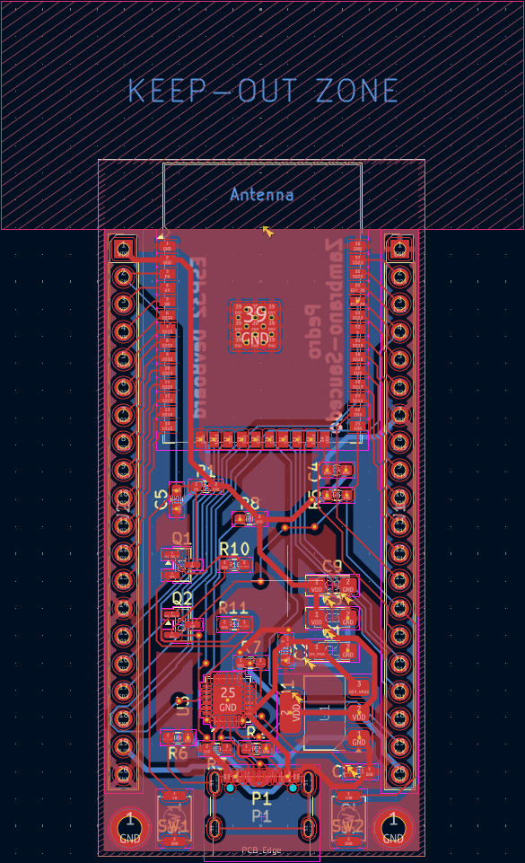 | 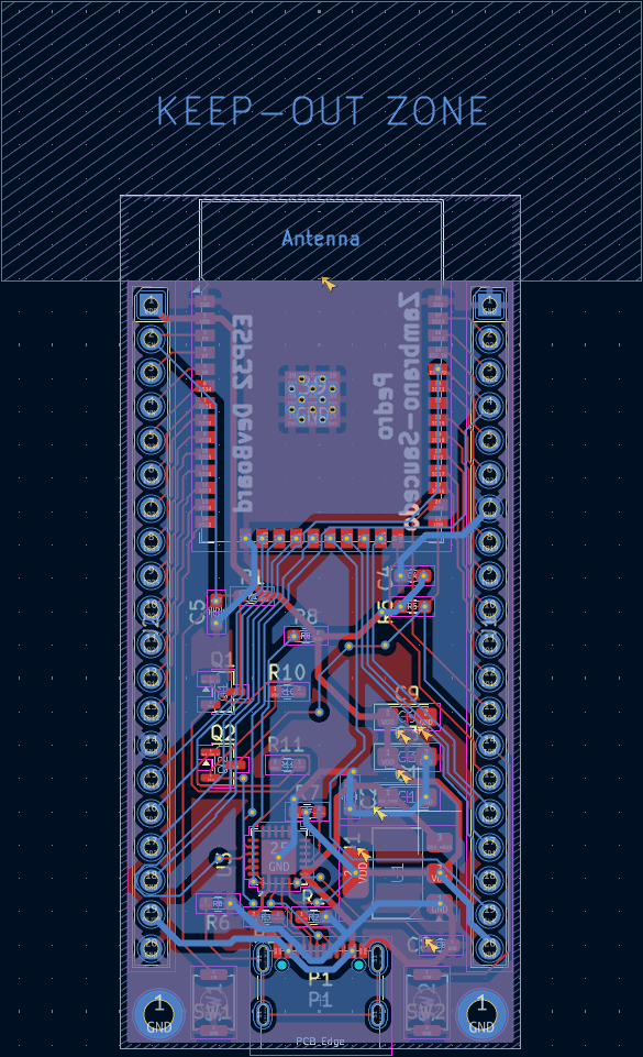 |
| Ref | Value | Footprint | Qty |
|---|---|---|---|
| U2 | ESP32-WROOM-32 | RF_Module:ESP32-WROOM-32 | 1 |
| U3 | CP2102N (e.g. CP2102N-A02-GQFN24) | QFN-24-1EP_4x4mm_P0.5mm_EP2.6x2.6mm | 1 |
| U1 | AMS1117-3.3 | SOT-223-3_TabPin2 | 1 |
| P1 | USB-C receptacle, 16-pin (GCT USB4105-GF-A) | USB_C_Receptacle_GCT_USB4105-xx-A_16P_TopMnt_Horizontal | 1 |
| Q1, Q2 | MMBT3904 | SOT-23 | 2 |
| C1, C3, C9 | 10 µF tantalum (C1 ≥ 16 V, C3/C9 ≥ 10 V) | CP_EIA-3216-18_Kemet-A_HandSolder | 3 |
| C2, C4, C8 | 100 nF | C_0603_1608Metric | 3 |
| C5 | 1 µF | C_0603_1608Metric | 1 |
| R1, R5, R7, R8, R10, R11 | 10 kΩ | R_0603_1608Metric | 6 |
| R2, R3 | 5.1 kΩ | R_0603_1608Metric | 2 |
| R6 | 1 MΩ | R_0603_1608Metric | 1 |
| SW1, SW2 | Tactile switch (Alps SKRK) | SW_Push_SPST_NO_Alps_SKRK | 2 |
| J1, J2 | 1×20 male header, 2.54 mm | PinHeader_1x20_P2.54mm_Vertical | 2 |
KiCad 9. Open hardware/Customized ESP-32.kicad_pro; open the schematic and board through the project so they stay linked.
hardware/
  Customized ESP-32.kicad_pro   project
  Customized ESP-32.kicad_sch   schematic (rev B)
  Customized ESP-32.kicad_pcb   board (rev B)
  Customized ESP-32.kicad_dru   custom design rules
  rev-a/                        original rev A schematic, kept for comparison
docs/images/                    renders, layout and schematic screenshots
Pedro Zambrano-Saucedo · Electrical Engineering, UTEP · Portfolio
| Qty | Value | Footprint | References |
|---|---|---|---|
| 6 | 10kΩ | Resistor_SMD:R_0603_1608Metric_Pad0.98x0.95mm_HandSolder | R1, R5, R7, R8, R10, R11 |
| 3 | 100nF | Capacitor_SMD:C_0603_1608Metric_Pad1.08x0.95mm_HandSolder | C2, C4, C8 |
| 2 | 10μF | Capacitor_Tantalum_SMD:CP_EIA-3216-18_Kemet-A_HandSolder | C1, C9 |
| 2 | 5.1kΩ | Resistor_SMD:R_0603_1608Metric_Pad0.98x0.95mm_HandSolder | R2, R3 |
| 2 | Conn_01x20_Pin | Connector_PinHeader_2.54mm:PinHeader_1x20_P2.54mm_Vertical | J1, J2 |
| 2 | MMBT3904 | Package_TO_SOT_SMD:SOT-23 | Q1, Q2 |
| 2 | SW_Push | Button_Switch_SMD:SW_Push_SPST_NO_Alps_SKRK | SW1, SW2 |
| 1 | 10µF | Capacitor_Tantalum_SMD:CP_EIA-3216-18_Kemet-A_HandSolder | C3 |
| 1 | 1MΩ | Resistor_SMD:R_0603_1608Metric_Pad0.98x0.95mm_HandSolder | R6 |
| 1 | 1µF | Capacitor_SMD:C_0603_1608Metric_Pad1.08x0.95mm_HandSolder | C5 |
| 1 | AMS1117-3.3 | Package_TO_SOT_SMD:SOT-223-3_TabPin2 | U1 |
| 1 | CP2102N-Axx-xQFN24 | Package_DFN_QFN:QFN-24-1EP_4x4mm_P0.5mm_EP2.6x2.6mm | U3 |
| 1 | ESP32-WROOM-32 | RF_Module:ESP32-WROOM-32 | U2 |
| 1 | USB_C_Receptacle_USB2.0_16P | Connector_USB:USB_C_Receptacle_GCT_USB4105-xx-A_16P_TopMnt_Horizontal | P1 |
The 26 most common of 28 parts.

mikes-techzone/upsy-desky
This repository contains the source files for the Upsy Desky, a device which lets you connect your standing desk to any home automation system.

PriyaUdhayakumar/Custom-ESP32-Development-Board
Custom-ESP32 Development Board-

beer88/PCB-Projects-Kicad
This repository contains a collection of PCB design projects developed using KiCad, covering a range of applications in embedded systems, automation, and hardware development.

Bellafaire/ESP32-Smart-Watch
An open source smartwatch based on the ESP32 compatible with the Arduino IDE.


It measures 30 × 64 mm and has 2 copper layers, 1.6 mm thick.
28 parts, built around the ESP32-WROOM-32, AMS1117-3.3 and MMBT3904. The full list of its parts is on this page, with links to each part's symbol and footprint where PCBKit's library has them.
From the pazambranosauc/esp32-devboard repository on GitHub, at the commit this page was made from: the board is hardware/Customized ESP-32.kicad_pcb and its schematic hardware/Customized ESP-32.kicad_sch. PCBKit opens the board in the browser, with nothing to install.
Its repository states no licence, so its author keeps all rights: ask pazambranosauc before reusing the design.