4 layers100 × 80 mm

 OutBlade/s6la81
Open-source 8-channel logic analyzer: FX2LP + Spartan-6, with a sigrok driver. Design in progress, not yet built or tested.
S6la8 is an open-source printed circuit board by OutBlade, from the OutBlade/s6la8 repository on GitHub. It is a 4-layer board of 100 × 64 mm with 155 parts on 172 nets, routed with 3,142 tracks and 734 vias.
It is built around the CY7C68013A-56PVXC, XC6SLX9-2TQG144C and SN74LVC245APWR(LX), with the TLV62569DBVR-TP, USBLC6-2SC6 and 24LC128-I/SN among its other parts. Its parts include 61 resistors, 58 capacitors, 14 ICs, 5 connectors and 4 diodes. It belongs with the sensors and measurement and fPGA and programmable logic boards and the FPGA and CPLD boards of this library.


An open-source 8-channel logic analyzer built around a Cypress/Infineon CY7C68013A (FX2LP) USB controller and a Xilinx Spartan-6 XC6SLX9 FPGA, with a driver for sigrok.
s6la8 is a working name.
The design files are complete and pass every check that can run without hardware. No board has been manufactured and no bitstream has been built yet, so build and test prototypes before ordering a batch (see docs/manufacturing.md).
| Part | State |
|---|---|
Schematic (hardware/s6la8.zen) | Complete, 155 parts. KiCad ERC: 0 errors; 7 "power pin not driven" findings are downgraded to warnings in the project file because the rails are fed by regulator outputs and the generated sheet has no power flags. Not yet reviewed by a second person |
PCB layout (hardware/eda/s6la8.kicad_pcb) | Fully routed. KiCad DRC: 0 errors, 0 unconnected, 1 warning (the probe header's silkscreen was trimmed at the board edge on purpose). Schematic parity: only naming differences. USB pair routed as a coupled 90 ohm pair. No signal- or power-integrity simulation |
Manufacturing package (hardware/release.py) | Gerbers, drill, JLCPCB BOM and pick-and-place, STEP, schematic and assembly PDFs, fab notes. Refuses to build unless DRC is clean |
Enclosure (case/) | Printable tray and lid (OpenSCAD), checked against KiCad's 3D model of the populated board: no collisions. Not yet printed |
FX2 firmware (firmware/) | Compiles with SDCC (4.0 KB of code). Never run |
FPGA gateware (gateware/) | Streaming, triggered capture into block RAM (32 K samples) or SDRAM (32 M samples), and board authentication pass simulation, the SDRAM against a model that checks the datasheet timing; Verilator lint clean; Yosys estimate 45 % of the LUTs. No ISE build yet, so pinout and timing are unverified |
libsigrok driver (host/driver/) | Compiles against libsigrok. Never run against a device |
Production tools (tools/) | Key generation, per-board provisioning and end-of-line test. Never run against a device |
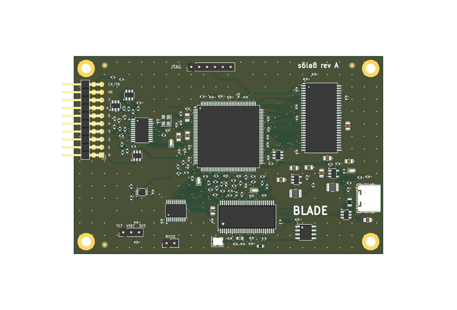
The schematic is in docs/schematic.pdf: one large generated sheet (2.7 x 1 m), best read zoomed in on screen.
fx2lafw analyzer with any
released sigrok, with the FPGA unconfigured.Rates implemented in gateware: up to 100 MS/s into the buffer, up to 25 MS/s streaming. 200 MS/s is a goal, not a feature.
The board is 100 x 64 mm, four layers (signal / GND / 3.3 V / signal). The flow is scripted and repeatable:
pcb layout hardware/s6la8.zen          # sync footprints and nets (Zener)
python layout/place.py eda/s6la8.kicad_pcb     # seed placement
python layout/route.py eda/s6la8.kicad_pcb     # Freerouting
python layout/fanout.py eda/s6la8.kicad_pcb    # plane vias
python layout/patch.py dump|rip|apply ...      # leftovers, see the file header
python layout/patch_solve.py ... # grid router with rip-up (needs numpy)(place.py, route.py, fanout.py and patch.py run with KiCad's bundled
Python.)
The leftover pass is a plain grid router. It closed the connections
Freerouting left open by cutting neighbouring tracks near a boxed-in pad and
joining them again around the new copper. The tracks it lays are legal but
not pretty (many short 0.05 mm jogs), and it moved parts of FD1, FD4,
FD7, FLAGA, SLOE, MODE, SD_BA0, SD_DQ1 and SD_DQ12 without any
regard for length or impedance.
layout/usb_pair.py re-routes the USB pair as a coupled pair and
layout/silk.py sets up the production silkscreen; both can run again after
pcb layout.
The leftover pass is a plain grid router. It closed the connections
Freerouting left open by cutting neighbouring tracks near a boxed-in pad and
joining them again around the new copper. One pin (FPGA pin 54, GND) needed a
placement change: decoupling capacitors C40 (1.2 V) and C46 (3.3 V) swapped
places so that the 1.2 V track no longer crosses the ground pin's exit. The
grid router's tracks are legal but not pretty, and it moved parts of FD1,
FD4, FD7, FLAGA, PKTEND, SLOE, MODE, SD_BA0, SD_DQ1 and
SD_DQ12 without regard for length; none of these is critical at the rates
implemented.
Before ordering a batch:
The FPGA bitstream checks that it runs on a board you provisioned:
tools/eol.py reads the DNA and writes
SipHash-2-4(key, DNA) into the EEPROM. The key is 128 bits from
tools/provision.py newkey and never leaves your machine.make -C gateware/ise bitstream PRODUCTION=1)
contains the key, recomputes the hash and refuses to capture if it does
not match. The sigrok driver says so plainly.Limits, and a decision for you. This repository is published under GPL and
CERN-OHL-S, which explicitly allow anyone to build and sell copies. The open
default build (auth_key_dev.vh) does not enforce the check, so a cloner can
simply build their own unrestricted bitstream from this repository. The
scheme only protects your product if the production gateware and key stay
private: keep gateware/ (you are its sole author, so you may relicense it)
and the key out of public repositories from now on, and protect the product
name with a trademark. The firmware is derived from fx2lafw and stays
GPL-2.0; the libsigrok driver stays GPL-3.0.
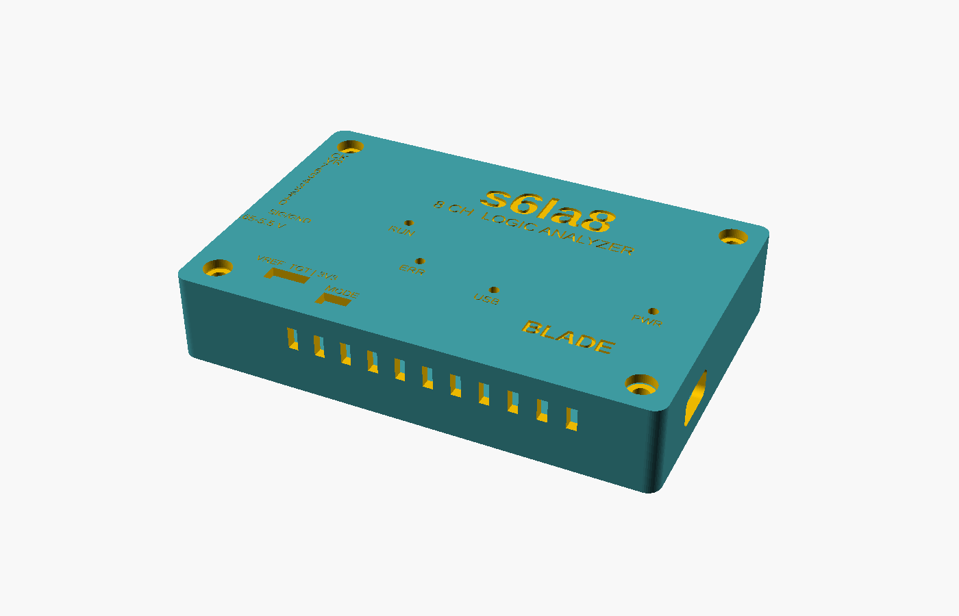
python hardware/release.py A # -> hardware/release/revA/Cost, supplier choice, import and the German legal requirements (CE, WEEE, packaging) for a run of 100 are in docs/manufacturing.md. The enclosure is in case/: PETG, no supports, four M3x12 screws into heat-set inserts.
Everything except the bitstream builds in the development container:
./dev.sh make -C firmware             # FX2 firmware -> firmware/build/s6la8-fx2.fw
./dev.sh make -C gateware sim lint    # simulation and lint
./dev.sh bash host/build.sh           # libsigrok with the s6la8 driver
On PowerShell use .\dev.ps1 instead of ./dev.sh.
The bitstream needs Xilinx ISE 14.7 WebPACK, which is x86-64 only (there is no open-source place-and-route for Spartan-6). On an x86-64 machine:
make -C gateware/ise bitstream # PRODUCTION=1 for the locked buildOn an Arm machine the same build runs in an x86-64 container; see gateware/ise/README-docker.md.
The hardware is described in Zener and
generates a KiCad 10 project in hardware/eda/. hardware/gen_pins.py
derives the FPGA pin constraints from the schematic.
The firmware currently uses the pid.codes test ID 1209:0001. That is for
development only and must be replaced by an assigned ID before any board is
distributed.
| Part | License |
|---|---|
host/driver/, gateware/ | GPL-3.0-or-later |
firmware/ | GPL-2.0-or-later (derived from sigrok-firmware-fx2lafw); bundled fx2lib is LGPL-2.1-or-later |
hardware/ | CERN-OHL-S-2.0 |
hardware/lib/ | Symbols and footprints copied from the KiCad libraries (CC-BY-SA 4.0 with the KiCad library exception) |
Full texts are in LICENSES/.
| Qty | Value | Footprint | References |
|---|---|---|---|
| 39 | 100nF 6.3V | stdlib_kicad-footprints_Capacitor_SMD:C_0402_1005Metric | C10, C11, C12, C13, C14, C15, C16, C17, C20, C21, C22, C23, C24, C25, C26, C27 +23 |
| 14 | 100k | stdlib_kicad-footprints_Resistor_SMD:R_0402_1005Metric | R1, R2, R3, R9, R11, R13, R15, R17, R19, R21, R23, R28, R40, R61 |
| 11 | 33 | stdlib_kicad-footprints_Resistor_SMD:R_0402_1005Metric | R7, R24, R29, R30, R31, R32, R33, R34, R35, R36, R43 |
| 10 | 100 | stdlib_kicad-footprints_Resistor_SMD:R_0402_1005Metric | R8, R10, R12, R14, R16, R18, R20, R22, R27, R60 |
| 9 | 10k | stdlib_kicad-footprints_Resistor_SMD:R_0402_1005Metric | R37, R38, R39, R41, R51, R52, R57, R58, R59 |
| 7 | 1k | stdlib_kicad-footprints_Resistor_SMD:R_0402_1005Metric | R25, R42, R45, R46, R47, R48, R54 |
| 5 | USBLC6-2SC6 | OutBlade_s6la8_lib:SOT-23-6 | U2, U3, U4, U5, U6 |
| 4 | 22uF 6.3V | stdlib_kicad-footprints_Capacitor_SMD:C_0805_2012Metric | C2, C3, C5, C6 |
| 4 | 4.7k | stdlib_kicad-footprints_Resistor_SMD:R_0402_1005Metric | R44, R49, R50, R53 |
| 4 | M3 DIN965 TopBottom | stdlib_kicad-footprints_MountingHole:MountingHole_3.2mm_M3_DIN965_Pad_TopBottom | H1, H2, H3, H4 |
| 3 | 10uF 10V | stdlib_kicad-footprints_Capacitor_SMD:C_0805_2012Metric | C1, C4, C29 |
| 3 | 4.7uF 6.3V | stdlib_kicad-footprints_Capacitor_SMD:C_0805_2012Metric | C18, C36, C44 |
| 3 | Fiducial | stdlib_kicad-footprints_Fiducial:Fiducial_1mm_Mask2mm | FID1, FID2, FID3 |
| 2 | 100nF 10V | stdlib_kicad-footprints_Capacitor_SMD:C_0402_1005Metric | C30, C37 |
| 2 | 10uF 6.3V | stdlib_kicad-footprints_Capacitor_SMD:C_0805_2012Metric | C28, C56 |
| 2 | 18pF | stdlib_kicad-footprints_Capacitor_SMD:C_0402_1005Metric | C57, C58 |
| 2 | 2.2k | stdlib_kicad-footprints_Resistor_SMD:R_0402_1005Metric | R55, R56 |
| 2 | 2.2uH | stdlib_kicad-footprints_Inductor_SMD:L_1210_3225Metric | L1, L2 |
| 2 | 5.1k | stdlib_kicad-footprints_Resistor_SMD:R_0402_1005Metric | R5, R6 |
| 2 | LED GREEN | stdlib_kicad-footprints_LED_SMD:LED_0603_1608Metric | D1, D3 |
| 2 | TLV62569DBVR | OutBlade_s6la8_lib:SOT-23-5 | U12, U13 |
| 1 | 1uF | stdlib_kicad-footprints_Capacitor_SMD:C_0402_1005Metric | C19 |
| 1 | 1uF 10V | stdlib_kicad-footprints_Capacitor_SMD:C_0402_1005Metric | C38 |
| 1 | 2.2uF 6.3V | stdlib_kicad-footprints_Capacitor_SMD:C_0603_1608Metric | C8 |
| 1 | 2.54mm 10 x 2 THT Horizontal Male | stdlib_kicad-footprints_Connector_PinHeader_2.54mm:PinHeader_2x10_P2.54mm_Horizontal | J3 |
| 1 | 2.54mm 2 x 1 THT Vertical Male | stdlib_kicad-footprints_Connector_PinHeader_2.54mm:PinHeader_1x02_P2.54mm_Vertical | J2 |
| 1 | 2.54mm 3 x 1 THT Vertical Male | stdlib_kicad-footprints_Connector_PinHeader_2.54mm:PinHeader_1x03_P2.54mm_Vertical | J5 |
| 1 | 2.54mm 6 x 1 THT Vertical Male | stdlib_kicad-footprints_Connector_PinHeader_2.54mm:PinHeader_1x06_P2.54mm_Vertical | J1 |
| 1 | 220 100MHz | stdlib_kicad-footprints_Resistor_SMD:R_0805_2012Metric | FB2 |
| 1 | 220 100MHz | stdlib_kicad-footprints_Resistor_SMD:R_0603_1608Metric | FB1 |
| 1 | 24LC128-I/SN | OutBlade_s6la8_lib:SOIC-8_3.9x4.9mm_P1.27mm | U1 |
| 1 | 24MHz 12pF | stdlib_kicad-footprints_Crystal:Crystal_SMD_3225-4Pin_3.2x2.5mm | Y2 |
| 1 | 330 | stdlib_kicad-footprints_Resistor_SMD:R_0402_1005Metric | R26 |
| 1 | 453k | stdlib_kicad-footprints_Resistor_SMD:R_0402_1005Metric | R4 |
| 1 | ASE-50.000MHZ-LC-T | OutBlade_s6la8_lib:Oscillator_SMD_Abracon_ASE-4Pin_3.2x2.5mm | Y1 |
| 1 | CY7C68013A-56PVXC | OutBlade_s6la8_lib:SSOP-56_7.5x18.5mm_P0.635mm | U11 |
| 1 | LED RED | stdlib_kicad-footprints_LED_SMD:LED_0603_1608Metric | D2 |
| 1 | LED YELLOW | stdlib_kicad-footprints_LED_SMD:LED_0603_1608Metric | D4 |
| 1 | MT48LC16M16A2P-6A | OutBlade_s6la8_lib:TSOP-II-54_22.2x10.16mm_P0.8mm | U14 |
| 1 | SN74LVC245APWR | OutBlade_s6la8_lib:TSSOP-20_4.4x6.5mm_P0.65mm | U7 |
| 1 | SN74LVC2T45DCUR | OutBlade_s6la8_lib:VSSOP-8_2.3x2mm_P0.5mm | U9 |
| 1 | SN74LVC8T245PWR | OutBlade_s6la8_lib:TSSOP-24_4.4x7.8mm_P0.65mm | U8 |
| 1 | USB4105-GF-A | OutBlade_s6la8_lib:USB_C_Receptacle_GCT_USB4105-xx-A_16P_TopMnt_Horizontal | J4 |
| 1 | XC6SLX9-2TQG144C | OutBlade_s6la8_lib:TQFP-144_20x20mm_P0.5mm | U10 |
It measures 100 × 64 mm and has 4 copper layers, 1.61 mm thick.
155 parts, built around the CY7C68013A-56PVXC, XC6SLX9-2TQG144C, SN74LVC245APWR(LX) and TLV62569DBVR-TP. The full list of its parts is on this page, with links to each part's symbol and footprint where PCBKit's library has them.
From the OutBlade/s6la8 repository on GitHub, at the commit this page was made from: the board is hardware/eda/s6la8.kicad_pcb and its schematic hardware/eda/s6la8.kicad_sch. PCBKit opens the board in the browser, with nothing to install.
Its repository states no licence, so its author keeps all rights: ask OutBlade before reusing the design.

frindaddy/digichiver
Archival hardware/firmware for the MM54104 Digitalker chip


PaulBichl/VibePCB-LA
A 16-channel, 100 MSa/s USB 2.0 HS logic analyzer: a Lattice ECP5 FPGA (CABGA-256 BGA) capturing into a 32 MB SDRAM (54-ball BGA), read out over an FT2232H. 98 x 64 mm, 6 layers.

GOROman/gbc-rp2350b-romcart
R0 review draft: RP2350B/Core2350B2 Game Boy cartridge carrier, KiCad/BOM/Gerber; not fabrication-ready

SmallCoral/c5-car
用 KiCad 10 打开 CoralC5-Expansion.kicadpro。这是 Coral-C5 的单槽扩展板,顶部 J14 接核心板,左右 J9、J8 各一组 2×24 排针,下方放 RJ45 和 microSD,右侧放 ESP32-C3-MINI-1U。100×86mm 板框为本项目暂定尺寸。

randomplum/autoliv_nv3_uvc
Adapter for the Autoliv NV3 sensor providing USB video device class output

Andreuxxx1977/esp32-p4
An open-hardware, actively cooled ESP32-P4 board for heavy multimedia work: a 2-lane MIPI camera, a 2-lane MIPI display, USB 2.0 High-Speed, 10/100 Ethernet, UHS-I microSD, 32 MB flash and 32 MB PSRAM.