6 layers50 × 50 mm
Osc dev m007
OpenServoCore/open-servo-core
The goal of this project is to create an open servo controller board and firmware.
100 parts39Apache-2.0

 OpenServoCore/open-servo-core39
The goal of this project is to create an open servo controller board and firmware.
Encoder board is an open-source printed circuit board by OpenServoCore, from the OpenServoCore/open-servo-core repository on GitHub, published under the Apache-2.0 licence. It is a 4-layer board of 25 × 25 mm with 10 parts on 6 nets, routed with 60 tracks and 68 vias.
Its parts include 4 resistors, 3 capacitors, 2 ICs and 1 connector. It belongs with the robots and motor control boards of this library.
Built and brought up. Rev. 2A board #1 runs an MG90 on 2S. Position calibration, the position table, motor identification and closed-loop verify all pass on it, and the sense chain is graded in Measured on board #1. Not exercised yet: the encoder inputs (J6 / J11), Qwiic, and the second position channel. Rev. 2A also stays open for value changes that need no routing change, so the BOM can still move; see Still open. Fabricate this at your own risk!
See CHANGELOG.md for revision history.
This is the OpenServoCore firmware development and validation board. It is built around the CH32V006F8P6 and designed to accept any gutted hobby servo (SG90, MG90, and similar), so firmware can be brought up and characterized against real motor / pot / encoder hardware.
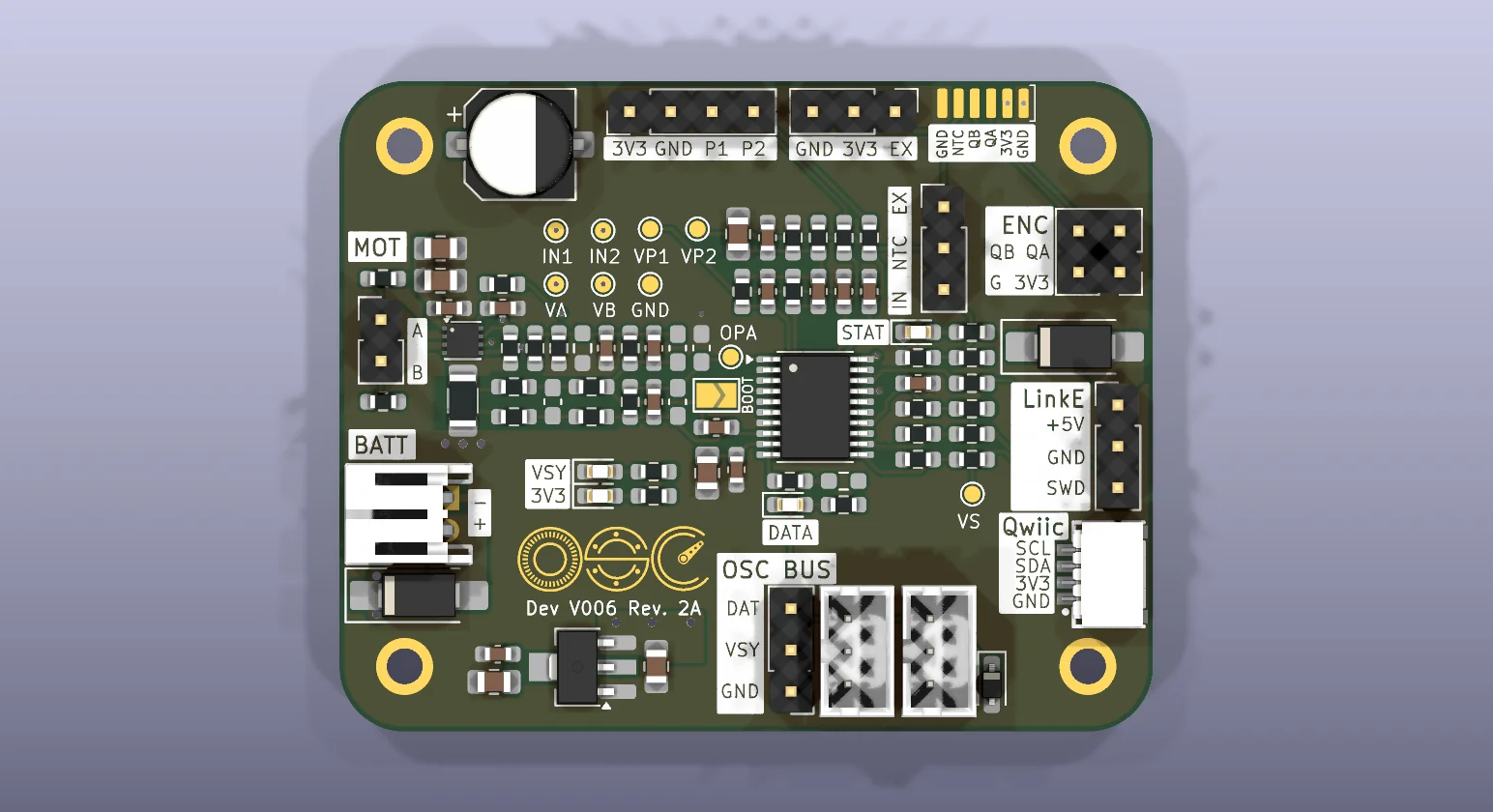
KiCad render of Rev. 2A.
PGND island and dumps heat through the prepreg into the ground plane, not into a copper plane of its own.+3V3 load at about 55 mA, board included, so keep add-ons on the 3V3 pins light and mind probe slips on the 3V3 headers. The DRV8212P VCC (+3V3_DRV) hangs off the same +3V3 as the MCU through Rh2, a fitted 0R that a ferrite can replace.PC0, wired straight to the MCU through a 33 Ohm series resistor. No buffer, no TX_EN. Direction turnaround and RX timing are firmware's job.DATA wire as bounded CRC'd bursts, so there is no second UART on the board.VSYS measured directly through its own divider, plus both motor terminals referenced to a common bias so back-EMF is readable while the bridge coasts.Rev. 2A is a big respin. Here is what changed:
DATA line connects straight to the MCU through a 33 Ohm series resistor (Rx1), and RX timing moved fully into firmware.VB) instead of GND, so both terminals stay readable during coast.VSNS is back, on its own pin, as a direct divider off VSYS.CH32V006F8P6, TSSOP20. The "Function used" column is what the board wires the pin for.
| Pin | Port | Net | Function used |
|---|---|---|---|
| 1 | PD4 | OPA_OUT | Op-amp output (OPO0). The same pin is ADC A7, which samples it. |
| 2 | PD5 | VSNA | ADC A5, motor terminal A sense. |
| 3 | PD6 | VSNB | ADC A6, motor terminal B sense. |
| 4 | PD7 | RST | nRST from the factory. After the option byte flip it becomes the op-amp + input (OPP1) through JP1. See First boot. |
| 5 | PA1 | VPOS1 | ADC A1, position channel 1: pot wiper or the first transducer output (RC-filtered). |
| 6 | PA2 | VPOS2_NTC | ADC A0, position channel 2 for a dual-transducer sensor, or the NTC divider when JP2 is jumped. |
| 7 | - | GND | VSS. |
| 8 | PD0 | OPA_N | Op-amp - input (OPN1), difference network summing node. |
| 9 | - | +3V3 | VDD. |
| 10 | PC0 | DATA | USART1 TX (remap 3), half-duplex (HDSEL) servo bus. Also TIM2 CH1 (remap 4) as the input of the bus break wake. |
| 11 | PC1 | SDA | I2C1 SDA, Qwiic (J3). |
| 12 | PC2 | SCL | I2C1 SCL, Qwiic (J3). |
| 13 | PC3 | DRV_EN | GPIO to the DRV8212P nSLEEP. A 10K pulldown (Rh1) keeps the driver asleep at reset. |
| 14 | PC4 | VSNS | ADC A2, VSYS supply divider. |
| 15 | PC5 | DRV_IN2 | TIM1 CH2 (remap 8), H-bridge PWM. |
| 16 | PC6 | DRV_IN1 | TIM1 CH3 (remap 8), H-bridge PWM. |
| 17 | PC7 | STAT | STAT LED, active low, driven as a plain GPIO. The only firmware-driven lamp. |
| 18 | PD1 | SWDIO | 1-wire debug, 100 Ohm series (Ru1) to J2. |
| 19 | PD2 | ENCB | Encoder B. ADC A3, analog quadrature sampling. |
| 20 | PD3 | ENCA | Encoder A. ADC A4, analog quadrature sampling. |
TIM1 runs center-aligned PWM on IN1/IN2 at 20 kHz, and its update event triggers the ADC scans at the counter crest and trough (see PWM and ADC timing). Remap 8 puts TIM1 CH4 on PC7, but CH4 is unused and STAT is a GPIO.
All 2.54 mm pin headers are vertical through-hole.
JST-PH 2P horizontal. 1S-2S LiPo only (3.0-8.4 V). The DRV8212P caps the safe motor rail at 11 V, so 3S is not supported. This input is OR'd into VSYS through an SS54 (Dp1), so it coexists with LinkE power.
1x03 pin header (2.54 mm) for the WCH-LinkE programmer / debugger.
| Pin | Net | Notes |
|---|---|---|
| 1 | VPROG | LinkE 5 V rail, OR'd into VSYS through an SS54 (Dp2). |
| 2 | GND | |
| 3 | SWDIO | 1-wire debug, through a 100 Ohm series resistor (Ru1). |
Three pins is the whole header now. Telemetry rides the servo bus, so the LinkE's TX / RX are not connected to anything.
Plugging in the LinkE alone is enough to power the board. Very handy for firmware-only sessions.
SH 1.0 mm 4P (GND / +3V3 / SDA / SCL), standard Qwiic pinout. 4K7 pull-ups (Rq1 / Rq2) sit on the MCU side, and 100 Ohm series resistors (Rq3 / Rq4) sit between the MCU and the connector.
This one is meant for an encoder module rather than generic sensors: an I2C magnetic encoder (MT6701 / AS5600 breakout) or a quadrature encoder adapter. The board has no hardware quadrature counting (see J6), so Qwiic is the flexible stand-in for it. I2C1 is polled.
1x02 pin header carrying MOT_A / MOT_B straight off the DRV8212P outputs. Through-hole, so the high-current path stays zero-via.
1x04 pin header, +3V3 / GND / POS1 / POS2. It takes:
POS1. Excitation comes from +3V3 and the wiper goes into POS1. Excitation and ADC reference share the same rail, so the reading is ratiometric and supply drift cancels out.POS1 and POS2. POS2 shares its ADC pin with the NTC, so leave JP2 open in this mode; the on-board temperature reading is given up for the second channel. Both channels sit behind identical 4K7 / 100nF filters (Ra1 / Ca1 and Ra2 / Ca2) so the pair stays phase-matched.With a pot or a single-output encoder, leave POS2 unconnected and jump JP2 for the NTC. For a digital magnetic encoder use Qwiic (I2C) instead.
2x02 pin header. +3V3 / GND on one row, ENCA / ENCB on the other, going into ADC channels A4 / A3. Silk reads QA / QB for the two phases.
This is a future expansion connector for an ADC-sampled custom IR quadrature encoder, in the style of ServoProject. The analog A/B phases get oversampled and interpolated for sub-count resolution. Hardware quadrature counting is not possible here since PD2 / PD3 don't carry TIM2 CH1/CH2, so I never considered it. A digital encoder belongs on Qwiic instead.
Six bare pads at 1.0 mm pitch for the motor-shaft encoder flex, attached tin-and-iron: the flex fingers are pre-tinned, laid on the pads and pressed with an iron, then hot glue over the pad row takes the strain. The footprint pair (Flex_Landing_1x06_P1.0mm on the board, Flex_Fingers_1x06_P1.0mm on the flex) lives in the shared library, and the same landing goes on the swap board, so the dev board rehearses the real attach. Pin 1 is at the bracket mark.
| Pin | Net | Notes |
|---|---|---|
| 1 | GND | Outer ground, guards the pair. |
| 2 | +3V3 | Emitter and phototransistor supply. |
| 3 | ENCA | IR sensor A, ADC A4. Same net as J6. Silk QA. |
| 4 | ENCB | IR sensor B, ADC A3. Same net as J6. Silk QB. |
| 5 | VNTC_EXT | Thermistor on the motor can, into the external leg of JP2. The divider resistor sits on the flex. Silk NTC. |
| 6 | GND | Outer ground. |
J6 and J11 are the same encoder input in two shapes: pins for a wired breakout or the bench coupon, the landing for the flex. Populate one.
1x03 pin header, VNTC_EXT / +3V3 / GND, for an external NTC thermistor or temperature sensor. Select it with JP2. The +3V3 pin is there so the external part can bring its own pull-up or supply: a bare thermistor divides against a resistor on the connector, a sensor with a driven output just takes the rail. Rn1 10K serves the internal TH1 leg only, so nothing on the board loads the external node. The firmware's NTC constants (10K pull-up, 10K / 3950 part) describe the onboard divider, so a bare 10K / 3950 thermistor on J7 takes the same conversion when a 10K from the J7 +3V3 pin to VNTC_EXT divides against it.
OpenServoCore talks over a single-wire half-duplex UART, the same electrical layer as a TTL servo bus. Three wires only (GND / V+ / DATA), the same pin count as a hobby servo cable. The wire protocol on top is osc-native, OSC's own break-framed protocol built for sub-$0.20 MCUs (spec).
Three connectors share the same nets. Pick whichever fits your wiring:
Pin order is G / V / D with V in the center, so a reversed bench header only swaps DATA and GND, never power.
The powered board feeds VSYS onto V+ to power downstream boards over the same cable. On the DATA line the order is connector, then ESD clamp (Dx1, PESD5V0L1BA), then the 33 Ohm series resistor (Rx1), then the pin. Rx1 is 33 Ohm rather than the usual 100 Ohm because DATA is the one line where edge speed matters at 3 Mbps over a whole chain, and the clamp does the protection work.
Rx2 is a DNP 10K pull-up footprint. The bus wants exactly one pull-up, at the host end, and servos self-bias internally, so populate Rx2 only when this board is the end of the wire on the bench. Board #1 runs with Rx2 fitted, on an osc adapter cable that carries DATA and GND only.
V+ is VSYS directly, unprotected. Anything you daisy-chain to the bus must tolerate the upstream board's full input voltage (up to 8.4 V at 2S full charge).
This jumper bridges the op-amp + input network (OPA_P) onto the shared nRST / OPP1 pin (PD7). It ships open on fresh boards and gets closed as the last step of first boot. Current sense is inactive until it is closed.
1x03 pin header, silk EX / NTC / IN. The center pin is the common signal routed to ADC A0 through Ra2 / Ca2. Jump it to either side, or leave it open:
NTC to IN uses the onboard Rn1 / TH1 divider.EX to NTC uses the external thermistor on J7.POS2 on J5) and there is no temperature reading.Motor return current flows through Rs1 (60 mOhm, 1 %, 50 ppm, 1206) between PGND and GND. Rs1 is the only tie between the two grounds, so every amp of motor return has to cross it. Net-tie kelvin taps (NT1 on the PGND pad, NT2 on the GND pad) feed the MCU's on-chip op-amp, which runs in bare mode behind an external four-resistor difference network.
VREF = 1.10 V (Rd1 1K6 from +3V3 over Rd2 1K6 in parallel with Rd3 1K6, decoupled by Cd1), so negative current from regen or reversal is visible too. The usable range is roughly -1.2 A to +2.3 A by design, the top set by the amplifier's output ceiling near VDD - 0.16 V. On board #1 the rest output sits about 0.15 V under VREF, the op-amp's input offset times its noise gain and inside the part's spec, which moves the range to about -1.1 A to +2.4 A. The offset drifts with board temperature (see Measured on board #1), so firmware measures the rest at boot and keeps tracking it whenever the shunt carries no current: torque off, a brake or coast, and the brake half of a slow-decay drive. The KiCad schematic lists Rd2 300 with Rd3 unfitted, a 0.52 V VREF and a -0.58 A to +2.9 A range; board #1 is built with 1K6 in both.OPA_P / OPA_N.Rk1 / Rk2 (fitted 0R) sit in series with the kelvin taps. They are swap points for gain-trim experiments: if they ever become real resistors, swap both to the same thin-film value or the arms go out of balance.
Precision money goes to the shunt (1 %, 50 ppm) and the Rf / Rg quad (0.5 %, 25 ppm thin film). Matching and drift are what limit accuracy there and firmware cannot compensate for either. Everything downstream is offset error and boot calibration eats it.
This is a swap-and-measure board, so the populated values are a starting point and a set of experiment footprints ship unpopulated (DNP):
| Ref | Value | Purpose when fitted |
|---|---|---|
Cc3 / Cc4 | 22 pF | Stack on the 22 pF comp caps for a slower, quieter corner (about 570 kHz). |
Ck1 | 100 pF | Differential filter across the kelvin pair, ahead of the gain resistors. |
Co1 | 22 pF | Load cap on the op-amp output. Layout insurance. PD4 is both the op-amp output and the ADC pin, so the cap sits straight on the output; keep it under the 50 pF load limit. |
Rx2 | 10K | DATA bus pull-up for single-device bench setups. |
The shunt itself has no alternate footprint. Other values (22 to 150 mOhm, all 1206) swap onto Rs1's own pads, so the kelvin taps never move. A second shunt in parallel would split the current by pad and trace resistance and break the symmetric entry, so there is no pad for one.
The DRV8212P's own OCP / TSD is the first protection layer. OCP trips at 4 A minimum, above the 2.3 A where the sense chain saturates and the 2.2 A firmware overcurrent trip under it, and a hobby motor stalls below it, so a hard stall lands on TSD first and the driver hiccups at about 1 Hz until firmware drops DRV_EN. OCP only fires on a shorted lead pair, in 4 us pulses the ADC will not see. V006 has no comparator units, so the rest is firmware: a kernel I2t limit drops DRV_EN and latches a stall fault that only the user can clear, IWDG covers hung firmware, and any reset kills the bridge through the Rh1 pulldown.
MOT_A / MOT_B go through Rv1 / Rv3 (6K4) into ADC A5 / A6, with Rv2 / Rv4 (1K6) and Cv1 / Cv2 (100 pF) returning to VB instead of GND.
VB is a 0.623 V bias node (Rb1 430 / Rb2 100 from +3V3, bulk Cb1 10uF and Cb2 100nF). The divider ratio is 0.20, so a tap reads 0.2 x terminal + 0.8 x VB:
PGND or a diode above VSYS. At -0.9 V the tap is still 0.32 V, and at 9.3 V it is 2.36 V, so neither phase clips.That is the point of the bias: both terminals stay readable while the bridge coasts, so vA - vB is real back-EMF rather than a rail-clamped stub. The rail comes back as 5 x tap - 4 x VB.
VB is read at boot with the driver parked. With the bridge Hi-Z no current flows in either leg, so both taps sit at VB itself and firmware recovers the bias with no extra pin. If the two taps disagree by more than 64 counts, the 773-count nominal stands in. The bias also shifts with drive current, since the divider bottoms inject into the VB node against its own 81 Ohm source impedance: about +80 mV at full duty on a 2S rail, which the 0.20 ratio turns into 0.3 V on a single-terminal reading. Firmware keeps the boot value and does not track that shift. The back-EMF path reads vA - vB, which is immune, and since both terminals are measured, a host that needs one terminal's absolute voltage under drive can correct VB from the two taps with one multiply-add.
Cv1 / Cv2 have one open option: 100 nF in place of 100 pF turns the taps into averaging taps, which would let the terminal read below the 160-tick floor (see Terminal voltage and back-EMF). The firmware would need an estimator that weights the crest and trough terminal samples by their ticks, and every consumer that reads the terminal at the PWM edge loses that view. Not decided; board #1 carries 100 pF.
VSYS has its own divider straight to GND: Rv5 6K4 / Rv6 1K6 with Cv3 100 pF, into ADC A2. Divide by 5, so 8.4 V lands at 1.68 V. Same reels and the same phase as the terminal dividers, so the two chains track each other and rail minus terminal resolves the bridge drop instead of disappearing into a ratio disagreement.
Two channels with the same filter. POS1 goes through Ra1 4K7 and Ca1 100nF into ADC A1. POS2 goes through Ra2 4K7 and Ca2 100nF into ADC A0, the node JP2 also drives, so it is either the second transducer output or the NTC, never both.
Rn1 10K pulls up against the onboard 10K / 3950 TH1 on the internal leg of JP2. JP2 routes that divider (or the external thermistor on J7) onto the shared A0 node, where Ca2 100nF is the filter for every source; Ra2 is only in the POS2 path.
Rev. 2A board #1 on a 2S LiPo, first against a 3.7 Ohm resistor grid (4.4 Ohm at J4 with its cable), then with an MG90 fitted. The grid figures come from notebook 10, which grades the chain against board D (the bodged Rev. B rig), and the back-EMF figures from notebook 11. The constants a capture is read with live in the dev-v006-2A entry of notebooks/oscnb/boards.py, and the ones the servo runs with in the board's main.rs. Those two are the authority; the tables below quote them. Source columns cite notebook sections as nb10 sec 8.
Ticks are 48 MHz TIM1 ticks (20.8 ns). The PWM half-period is 1200 ticks, so a drive window of h ticks is h / 1200 duty.
| Item | Value | Source |
|---|---|---|
| PWM | Center-aligned, ARR 1200 at 48 MHz, 2400 ticks a period: 20 kHz. | servo-ch32/src/cfg/chip.rs |
| ADC clock | 24 MHz (HCLK / 2). | servo-ch32/src/hal/clocks.rs |
| Aperture | 13.5 ADC clocks on every channel. A conversion is 26 clocks: 1.083 us, 52 ticks, 0.92 Msps. | cfg/chip.rs, nb10 sec 8 |
| Trigger | TIM1 update (TRGO) at the counter crest and at the trough, so two scans a period. TIM1 CH4 (CCR4 = ARR - 68) starts the low-side tap's injected conversion before the crest: tap B forward, tap A reverse. | providers/sensors/scan.rs |
| Scan order | shunt, high tap, low tap, pos, vref, vbus, ntc: vmA before vmB forward, vmB before vmA reverse. The order follows a direction flip one period late. | main.rs, providers/sensors/scan.rs |
| Sample closes from the crest | Low-side tap -37 (injected), shunt +31, high-side tap +83; the scan's own low-side tap +135, read only from the trough scan (Fast decay). The same in both directions. The ADC's 2-clock trigger delay included. | nb10 sec 8, bringup captures/winding-r/injb |
Under slow decay the drive window is centred on the crest, so the crest scan reads the driven half; under fast decay the trough scan does.
Why 24 MHz, not 48. With the ADC's low-power comparator buffer on, a bit trial at 48 MHz gets 20.8 ns and the buffer does not settle. A pot sweep on board D reported 63% of the codes the wiper crossed at 48 MHz against 96% at 24 MHz, with the 55 codes under 1024 unreachable. The aperture cannot shrink either: 3.5 and 7.5 clocks run a slot at 1.5 and 1.2 Msps, which datasheet Table 3-23 rates only from VDD 4.5 V, and the MCU rail here is 3.3 V.
| Quantity | Design | Board #1 | Source |
|---|---|---|---|
| Scale | 1108.5 counts/A, 0.902 mA per count | Amplifier and ADC +0.5% (-0.7 to +2.3%): 93-94 mV on a meter across Rs1 during a 100% grid lap, against 93.3-95.1 mV from the chip's current times 60 mOhm. | boards.py current_chain_scale_measured, nb10 sec 7 |
| Rest output | 1.10 V (VREF) | About 0.15 V under VREF torque off at room temperature: 0.37 V over the schematic's 0.52 V VREF. Offset, tracked by firmware. | board #1 bringup |
| Rest drift | - | Normal mode: 1178 counts at 28 C, 1174 at 44 C, 1170 at 60 C, about -0.25 counts/C. High-speed mode, measured earlier over the 0.52 V VREF: 467 counts at 28 C, 398 at 43 C, 260 at 60 C. The on-chip op-amp has no drift spec. | board #1 bench |
| In-drive zero | - | 10 counts over the torque-off rest: the DRV8212P's own supply current returns through Rs1 once the driver wakes. | nb11 sec 1 |
| Rest noise | - | 1.28 counts RMS (1.15 mA). Board D 1.7. | rest_current_noise_measured, nb10 sec 3 |
| Step response | - | Half-way 48 ticks (1.00 us) after the ON compare, then a 13.1-tick (273 ns) exponential and a slow tail, 3.3% at half-way +48 ticks and 0.7% at +96. High-speed mode was 44 ticks, 10.1 ticks and 2.6%, with the same 0.7%. Steepest about 2.4 V/us. | bringup captures/winding-r/c0 bursts, shunt over the terminal difference |
| Settled to 1% | - | 156 ticks (3.25 us) after the ON compare, always approached from below. Measured in high-speed mode; normal mode's tail matches it within 0.1% from 130 ticks. | shunt_settle_measured |
| Crest honest to 3% | - | From 7% duty on the 2S grid. Board D 15%. | crest_floor_measured, nb10 sec 5 |
| ON pulse against the command | DRV8212P dead time 500 ns (24 ticks) typ | 30 ticks short at half height on the grid. On the MG90, 10-15 ticks short at about 0.1 A and 20-25 at 0.2 A and up. | nb10 sec 8.1, nb11 sec 4 |
Op-amp temperature. The op-amp runs in its normal mode. High-speed mode is off in firmware with no switch to turn it on: it gives up the factory offset trim (WCH AN24000), and on board #1 that cost more than the bandwidth bought. Board #1 drove the 3.7 Ohm grid at four DC levels, 54 to 99 mV across Rs1 on a meter, at room (28 to 30 C board), 44 C and 60 C, then at room again, once per mode. The data is captures/winding-r/c0 in the osc-dev-v006-bringup repo.
| Mode | Gain, room to 60 C | Zero, torque off | In-drive offset |
|---|---|---|---|
| Normal | -0.26%, back within 0.1% at room again | 1178 to 1170 counts | About +10 counts, steady |
| High-speed | +0.8% at 44 C, +4.3% at 60 C | 1106 to 916 counts | 21 counts at room to 46 at 60 C, level-dependent |
High-speed mode bends above 43 C. In normal mode the meter reads 1110.9 counts/A through zero at room, +0.22% on the 1108.5 design. Counts per level fall 0.4% from 54 to 99 mV, which looks like compression but is the +10-count step between the torque-off zero and the in-drive zero (see In-drive zero above), spread over the levels by a fit through the torque-off zero. The winding-R ladder holds within 1% of its 30-40% reference from 15% duty and within 3% from 10%, in both modes at every temperature: tap B's sample timing sets that floor, not the op-amp. A firmware change to the tap sampling is in progress.
Window floor. The firmware reads a current only when the drive window is at least i_window_min_ticks wide. Uncorrected, the grid's crest sample reads low under every floor, never high. In normal mode, from the high-speed grid ladder (nb10 sec 8.2) times the measured ratio between the modes:
| Within | Window | Duty |
|---|---|---|
| 1% | 125 ticks | 10.4% |
| 2% | 88 ticks | 7.3% |
| 3% | 72 ticks | 6.0% |
| 5% | 58 ticks | 4.8% |
The board runs at 64 ticks (5.3% duty): a slightly low reading beats no reading. On top of that, i_settle_gain multiplies every window-valid current by the inverse of the step response at its sample instant, in 21 Q15 bands of 8 ticks from 40 ticks (x1.133) to 208, unity past that. In normal mode the grid ladder reads about 4.5% low at 60 ticks and 1.1% at 120, settled from about 208, the same in both drive signs. The table is the high-speed one, which put every grid rung from 60 to 300 ticks within 0.16%, times the ratio between the modes; that predicts every rung from 64 ticks within 0.5%. Telemetry's current_raw and current_trough and the bias tracker stay raw.
Two things the gain cannot remove:
bias_brake_min_ticks, up to 20% duty), because the amplifier's tail after a pulse holds a shorter trough above rest. That tail was measured on board D and carried over.| Quantity | Board #1 | Source |
|---|---|---|
| Tap difference | 4.028 mV at the terminals per count of vA - vB (r = 5), bias free. | boards.py |
| One terminal | 5 x tap - 4 x VB in counts. A driven-low terminal reads 618 counts, not 0. | boards.py term_v, nb11 |
VB at rest | Taps 769.8 and 771.0 counts against 772.8 nominal (tap A 620 mV). | nb10 sec 3 |
VB under drive | With tap B disconnected from its terminal, it read the node itself: +68 mV (84 counts) at the forward 100% rung, against +67 mV from the 81 Ohm source. | nb10 sec 9 |
| Tap A rest noise | 0.86 counts, 3.5 mV at the terminal. | nb10 sec 3 |
| Low-side path | 0.218 Ohm on the A side: switch, shunt and copper. | nb10 sec 5.1 |
| Window edge | The terminal starts to fall 8.5-9 ticks after the OFF compare. The high-side tap at +83 reads the window from about 74 ticks, the injected low-side tap from about 90, the trough scan's low-side tap from about 126. | nb10 sec 8.4, bringup captures/winding-r/injb |
| Coast EMF | 1.24 mV per ripple Hz both ways on the MG90. Board D 1.21-1.23. | nb11 sec 3 |
| Low-duty over-read | The 15% rung reads 3.0% (forward) and 3.6% (reverse) high against a Ke fitted on 25-30%. Board D 7.7-7.8% on the same motor. | nb11 sec 3 |
v_window_min_ticks is 93 (7.7% duty). The low-side tap is sampled 37 ticks before the crest, so the floor is its rise after the ON edge: on the grid, forward drive reads R within 1.1% from 84 ticks, against 3.8% high at 96 when tap B sat in the scan's third slot. Reversed, with tap B sampled early as the high side, the same ladder read 3-5% high from 96 to 180 ticks against the 30-40% rungs: the early sample catches the high side's post-edge overshoot. So the taps swap with the drive direction, the low side always early and the high side always at +83, and the same ladder then reads R within 0.9% from 96 ticks in both directions. Fast decay keeps 160 (v_trough_window_min_ticks), its low-side tap still in the trough scan. The coast reading says the terminal chain reads the EMF as well as board D's; the low-duty over-read is the drive pulse coming out shorter than commanded, which a crest sample cannot see (11-16 ticks explains all of it on the MG90). The back-EMF observer keeps its own 160-tick floor (bemf_window_min_ticks) until it takes that shortfall off the commanded width; under it the back-EMF is void, which is why closed-loop verify's velocity legs, at 8-11% duty, run on the pot observer.
| Quantity | Board #1 | Source |
|---|---|---|
VSNS scale | Ratio 5 (Rv5 6K4 / Rv6 1K6 to GND): 4.028 mV at VSYS per count. | main.rs, boards.py |
| Pack voltage | VSYS + 0.25 V at rest, the firmware's rail_drop_mv for the SS54. | main.rs |
| 2S under load | 7.73 V at rest, 7.40 V at the grid's 100% rung: 0.21 Ohm of pack, diode and wiring. | nb10 sec 7 |
| Rest noise | 3.8 mV. | nb10 sec 3 |
TH1 (10K / 3950 to GND) under Rn1 10K reaches A0 with JP2 on NTC-IN. An external 10K / 3950 on J7 reads the same way under a 10K pull-up to +3V3, with JP2 on EX-NTC. Firmware publishes ntc_raw counts only, and the host converts:
R = 10K x raw / (4095 - raw), T = 1 / (1 / 298.15 K + ln(R / 10K) / 3950) - 273.15 °C
as ntc_c in oscnb/thermal.py does. An external NTC taped to the MG90's can logged it every minute through the overnight rest series in notebooks/telemetry/mg90-a__dev-v006-2A__2s__rest (ambient.csv.gz).
The pot is ratiometric on VDD, so reference drift cancels, and the 24 MHz ADC clock above is what keeps the pot's codes (96% of those crossed, against 63% at 48 MHz). Calibration, the position table and identification are per servo and stored on it. On board #1 the MG90's table moves slowly with running (notebook 12), so recalibrate from time to time.
VDD on board #1 is not metered. Absolute volts and amps use the declared 3.300 V; board D measured 3.28 V.POS2.Passives are numbered by the net they serve, not by the sheet they are drawn on. One letter means one thing across R, C and D, so Rv1 and Cv1 are part of the same divider. U, J, JP, TP, NT, TH, H and LOGO keep plain numbers.
| Letter | Family | Examples |
|---|---|---|
f | OPA feedback | Rf1, Rf2 |
g | OPA gain | Rg1, Rg2 |
c | OPA compensation | Cc1 - Cc4 |
i | OPA input | Ci1 |
o | OPA output | Co1 |
d | VREF divider | Rd1 - Rd3, Cd1 |
k | Kelvin taps | Rk1, Rk2, Ck1 |
s | Shunt | Rs1 |
v | Terminal and supply dividers | Rv1 - Rv6, Cv1 - Cv3 |
b | VB bias | Rb1, Rb2, Cb1, Cb2 |
n | NTC | Rn1 |
p | Power input and LDO | Cp1 - Cp3, Dp1, Dp2 |
l | Lamps (LEDs and their resistors) | Dl1 - Dl4, Rl1 - Rl4 |
u | MCU supply and debug | Cu1, Cu2, Ru1 |
q | Qwiic I2C | Rq1 - Rq4 |
h | H-bridge | Ch1 - Ch5, Rh1, Rh2 |
a | Angle sensor (pot) | Ra1, Ca1 |
x | One-wire bus | Rx1, Rx2, Dx1 |
All four are deliberately dim, in the 0.1-0.3 mA class.
| LED | Ref | Color | Meaning |
|---|---|---|---|
VSYS | Dl1 | yellow | System rail present. |
3V3 | Dl2 | green | Logic rail up. |
DAT | Dl3 | blue | Servo bus activity (active low). Passive lamp on the DATA line, no firmware involved. At the schematic's 4K7 (Rl3) it is faint on board #1; 1K is the brighter swap. |
STA | Dl4 | red | Servo health (PC7, active low), never traffic. In precedence order: lit for a 150 ms lamp test at boot, solid while a fault is latched (until the torque ack clears it), a 1 Hz blink while data_flags names a reason closed loop is refused (not calibrated, plant unset, stamp mismatch), dark when healthy. |
Nine 1.0 mm probe pads, labeled on silk. Seven sit in two rows between the position header and the sense network; OPA sits beside the MCU on the op-amp output, and VS beside the LinkE header. They take a scope tip or a pogo pin; nothing clips on, so for hands-free capture solder a wire loop to the pad.
| Silk | Ref | Net | What it is |
|---|---|---|---|
GND | TP1 | GND | Ground for the two-row group. |
OPA | TP2 | OPA_OUT | Op-amp output, ADC A7. Inline on the trace into PD4. |
IN1 | TP3 | DRV_IN1 | H-bridge PWM input 1 (PC6, TIM1 CH3). |
IN2 | TP4 | DRV_IN2 | H-bridge PWM input 2 (PC5, TIM1 CH2). |
VA | TP5 | VSNA | MOT_A divider tap, ADC A5. Inline on the trace into PD5. |
VB | TP6 | VSNB | MOT_B divider tap, ADC A6. Inline on the trace into PD6. Not the bias node VB, which is probed at Cb2. |
VS | TP7 | VSNS | VSYS divider tap, ADC A2. |
VP1 | TP8 | VPOS1 | Position channel 1 after its RC filter, ADC A1. |
VP2 | TP9 | VPOS2_NTC | Position channel 2 or the NTC divider after its RC filter, ADC A0. Follows JP2. |
OPA, VA and VB are in the signal path, so the pad adds no stub to those nets. The rest are short spurs off filtered or driven nodes. VREF has no pad: probe across Rd3. The kelvin pair ISNS+ / ISNS- has no pad on purpose. The 4x M2 mounting holes (2.2 mm) are tied to GND for an alligator clip.
Battery (VBAT) and LinkE 5 V (VPROG) OR into VSYS through Dp1 / Dp2. The SS54s drop about 0.25 V at rest (the firmware's rail_drop_mv, which a host adds back to VSYS for the pack voltage), and they block regenerated current from flowing back into either supply. VSYS is the raw motor rail and also feeds the LDO. +3V3 is logic and, through Rh2, the DRV8212P VCC (+3V3_DRV). Rh2 ships as 0R; it is the swap point for a ferrite (600 Ohm at 100 MHz) if driver noise ever shows on the MCU rail, which is also the ADC reference.
The bridge decoupling (Ch1 100nF on +3V3_DRV, Ch2 100nF plus Ch3 / Ch4 10uF plus Ch5 100uF on VSYS) returns to GND, not PGND. That is deliberate. At PWM timescales the motor current loops cap to bridge to motor to PGND and back to the cap. If those caps landed on the PGND side, the loop would close without crossing the shunt and the ADC would only see average draw instead of the real chopped current.
PGND is a tiny top-layer island: the driver's GND pins and thermal pad, Rh1, NT1, and the PGND side of the shunt. Nothing else.
Use a WCH-LinkE on J2. The link talks the CH32V006's 1-wire protocol on SWDIO.
The MCU's nRST and the op-amp + input share pin PD7. Fresh chips come out of the factory with RST_MODE=10, so the pin is reset, and the sense network parks it near GND, which would hold the MCU in reset if it were connected. JP1 breaks the link until the option byte is flipped:
RST_MODE=11 so PD7 becomes a GPIO.Do not close JP1 early. On an unprovisioned chip the op-amp network holds the pin near GND and the chip sits in reset. Recovery is reopening the jumper.
After this, the board runs as designed and current sense is live.
| Qty | Value | Footprint | References |
|---|---|---|---|
| 2 | 100 | Resistor_SMD:R_0805_2012Metric_Pad1.20x1.40mm_HandSolder | R2, R4 |
| 2 | 100nF | Capacitor_SMD:C_0805_2012Metric_Pad1.18x1.45mm_HandSolder | C1, C2 |
| 2 | 33K | Resistor_SMD:R_0805_2012Metric_Pad1.20x1.40mm_HandSolder | R1, R3 |
| 2 | ITR1204SR10A_TR(BY) | shared:OPTO-SMD-4_ITR1204SR10A | U1, U2 |
| 1 | 10uF | Capacitor_SMD:C_0805_2012Metric_Pad1.18x1.45mm_HandSolder | C3 |
| 1 | Conn_01x04 | Connector_PinHeader_2.54mm:PinHeader_1x04_P2.54mm_Vertical | J1 |
It measures 25 × 25 mm and has 4 copper layers, 1.6 mm thick.
10 parts. The full list of its parts is on this page, with links to each part's symbol and footprint where PCBKit's library has them.
From the OpenServoCore/open-servo-core repository on GitHub, at the commit this page was made from: the board is hardware/boards/encoder-board/encoder-board.kicad_pcb and its schematic hardware/boards/encoder-board/encoder-board.kicad_sch. PCBKit opens the board in the browser, with nothing to install.
Its repository publishes it under the Apache-2.0 licence: you may reuse it on that licence's terms (keep the author's notice, and for a copyleft licence share your changes alike).
OpenServoCore/open-servo-core
The goal of this project is to create an open servo controller board and firmware.

OpenServoCore/open-servo-core
The goal of this project is to create an open servo controller board and firmware.

OpenServoCore/open-servo-core
The goal of this project is to create an open servo controller board and firmware.

OpenServoCore/open-servo-core
The goal of this project is to create an open servo controller board and firmware.

OpenServoCore/open-servo-core
The goal of this project is to create an open servo controller board and firmware.


nanographs/Open-Beam-Interface
Just what you need to control the beam and get an image.


clydeshaffer/gametank
design files for the gametank hardware implementation

lukasloetkolben/OpenpilotHardware
Welcome to the Openpilot Hardware Collection!

COVESA/Open1722
Open-source implementation of the IEEE 1722 protocol, for streaming audio/video, tunneling CAN/LIN messages and enabling remote access to peripherals

system76/thelio-io-hardware
KiCad electrical design of Thelio Io board
