2 layers107.5 × 62 mm
 OpenScienceTools/DI-Lambda
DI-Lambda spectrophotometer
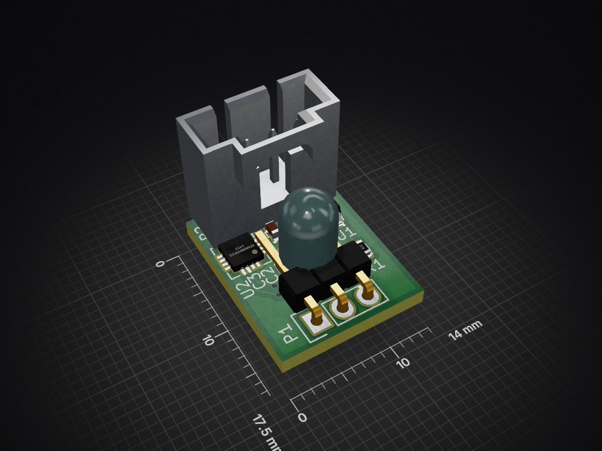
LED Board Module is an open-source printed circuit board by OpenScienceTools, from the OpenScienceTools/DI-Lambda repository on GitHub. It is a 2-layer board of 14 × 17.5 mm with 12 parts on 14 nets, routed with 93 tracks and 7 vias.
Its parts include 2 capacitors, 2 ICs, 2 connectors, 1 resistor and 1 diode. It belongs with the Silicon Labs (EFR32, EFM) boards of this library.
| Qty | Value | Footprint | References |
|---|---|---|---|
| 1 | 100nF | Capacitors_SMD:C_0603 | C3 |
| 1 | 1uF | Capacitors_SMD:C_0603 | C2 |
| 1 | 96R | Resistors_SMD:R_0603 | R1 |
| 1 | BCR42XU | SOT26 | U1 |
| 1 | C2CK | Footprints:TEST_POINT | W7 |
| 1 | C2D | Footprints:TEST_POINT | W8 |
| 1 | CONN_01X03 | Pin_Headers:Pin_Header_Straight_1x03 | P1 |
| 1 | CONN_01X04 | Pin_Headers:Pin_Header_Straight_1x04 | P2 |
| 1 | EFM8BB10F2G | Footprints:Silabs-QFN20 | U2 |
| 1 | LED | LEDs:LED-5MM | D2 |
| 1 | RX | Footprints:TEST_POINT | W6 |
| 1 | TX | Footprints:TEST_POINT | W1 |
It measures 14 × 17.5 mm and has 2 copper layers, 1.6 mm thick.
12 parts. The full list of its parts is on this page, with links to each part's symbol and footprint where PCBKit's library has them.
From the OpenScienceTools/DI-Lambda repository on GitHub, at the commit this page was made from: the board is schematics/LED-Board-Module/LED-Board-Module.kicad_pcb. PCBKit opens the board in the browser, with nothing to install.
Its repository states no licence, so its author keeps all rights: ask OpenScienceTools before reusing the design.


github-linguist/linguist
Language Savant. If your repository's language is being reported incorrectly, send us a pull request!


google/mozc-devices
Circuit diagrams and firmware source code for Gboard DIY keyboards


hackclub/OnBoard
💡 Join 1,000 teenagers and make your first PCB with a $100 grant!

VoronDesign/Voron-Tap
Tap is a nozzle-based z-probe for the V2 and Trident printer designs. The entire toolhead moves to trigger an optical switch. Tap offers many advantages:

stacksmashing/pico-tpmsniffer
A simple, very experimental TPM sniffer for LPC bus