4 layers275 × 240 mm
 Omkar1464/Telemetry-Module-using-CDMA-Modulation
This repository contains the embedded firmware, circuit schematics, simulation models, and validation benchmarks for the Long Range Telemetry Module (Phase-I) designed for high-altitude drone and UAV/CanSat payload…
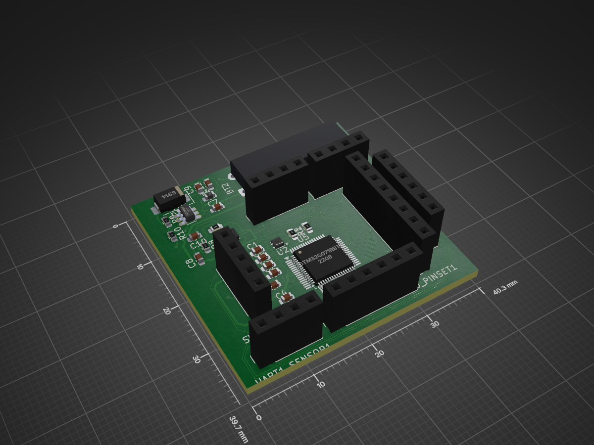
Power circuit new is an open-source printed circuit board by Omkar1464, from the Omkar1464/Telemetry-Module-using-CDMA-Modulation repository on GitHub. It is a 2-layer board of 40.3 × 39.7 mm with 32 parts on 69 nets, routed with 432 tracks and 15 vias.
It is built around the STM32G071RBT6, MCP1640-I/MC and MT3608, with the SS14 among its other parts. Its parts include 11 capacitors, 6 resistors, 4 ICs, 2 inductors and 1 diode. It belongs with the STM32 boards of this library.






B.Tech Phase-I Project Report & Codebase
Department of Electronics Engineering, Sardar Vallabhbhai National Institute of Technology (SVNIT), Surat
Academic Year: 2025–26 | Project Group: G60
Project Guide: Dr. Suresh Dahiya (Assistant Professor, DoECE)
Authors: Moksha Parikh (U23EC001), Ridham Chaudhary (U23EC030), Omkar Sinh (U23EC048)
This repository contains the embedded firmware, circuit schematics, simulation models, and validation benchmarks for the Long Range Telemetry Module (Phase-I) designed for high-altitude drone and UAV/CanSat payload communication.
Operating under the severe resource constraints of an 8-bit ATmega328P microcontroller (16 MHz clock, 2 KB SRAM), the system implements a Direct Sequence Spread Spectrum (DSSS) / Code Division Multiple Access (CDMA) baseband transmitter alongside a discrete 433 MHz RF front-end architecture.
                       +------------------------------+
                       |      2.5V - 3V Battery       |
                       +--------------+---------------+
                                      |
                            [DC-DC Boost Converter]
                                      |
                 +--------------------+--------------------+
                 | (3.3V / 5V Logic)                       | (Vcc RF)
                 v                                         v
+------------------------------------+    +----------------------------------+
|           Sensors & Inputs         |    |        Discrete RF Chain         |
| - u-blox NEO-6M GPS (UART @ 9600)  |    | - MPSH10 Colpitts LO (~358 MHz)  |
| - SHT-40 Humidity & Temp (I2C)     |    | - Dual BF998 MOSFET Mixers       |
| - PT1000-S Platinum RTD (I2C)      |    | - SAW Filter FL1 (433.92 MHz)    |
| - On-board NTC Thermistor (ADC)    |    | - RD01MUS2B RF Power Amplifier   |
+-----------------+------------------+    | - Pi-Matching Network & SMA Port |
                  |                        +-----------------+----------------+
                  v                                          ^
+------------------------------------+                       |
|       ATmega328P Controller        |                       |
| - LFSR PRN Generator (10-bit)      |                       |
| - 8x Bit-Packed Memory Storage     |                       |
| - Single-Cycle Port Writes (DPM)   |                       |
+--------+--------------------+------+                       |
         | (Dout-1: I-Chan)   | (Dout-2: Q-Chan)             |
+--------------------+------------------------------+| Folder / File | Description |
|---|---|
GPS-Neo6M/ | Arduino firmware for NEO-6M GPS NMEA sentence extraction, checksum validation, and coordinate parsing using TinyGPS++. |
I_trail/ & I_trial1/ | Baseband firmware implementation for the I-Channel (1000-chip LFSR generation, bit-packing, cycle-accurate delay loops). |
Q_trail/ | Baseband firmware implementation for the Q-Channel (10-chip array spreading code, corrected timing loops). |
task1/ & task2/ | Firmware test suites, sensor serialization routines, and hardware debugging logs. |
BF998 MOSFET LIB/ | Spice simulation libraries and component footprints for the BF998 dual-gate N-channel MOSFET. |
Datasheet/ | Technical documentation and datasheets for active and passive components (MPSH10, BF998, RD01MUS2B, NEO-6M, SHT-40). |
CDMA transferring rate.pdf | Documentation on CDMA transmission speed, spreading factors, and modulation characteristics. |
G48- Update-LO Simulation... | Report and simulation data for the Local Oscillator circuit. |
Design1.ms14 | NI Multisim top-level schematic and RF modulator simulation circuit. |
L_oscillator.ms14 | NI Multisim Colpitts oscillator simulation model. |
d2.ms14 & d2out.scp | Multisim circuit simulation and oscilloscope graph captures. |
oscillator.cir | SPICE netlist for the Colpitts Local Oscillator stage. |
The ATmega328P has only 2 KB of SRAM. Allocating 1000 chips as individual uint8_t bytes would consume 1000 bytes (almost 50% of total SRAM):
uint8_t I_CDMA_PACKED[125]).0x02DF, eliminating large hardcoded arrays in flash memory.digitalWrite() requires ~50–60 clock cycles.PORTB, changing pin states in a single clock cycle ($62.5\text{ ns}$ at $16\text{ MHz}$):
PORTB |=  (1 << PORTB2); // Set Pin 10 HIGH (1 cycle)
PORTB &= ~(1 << PORTB2); // Set Pin 10 LOW (1 cycle)Timer0) introduces up to $2\ \mu\text{s}$ interrupt jitter every $1.024\text{ ms}$. This is eliminated by calling noInterrupts() before entering the continuous transmission loop.To achieve a target chip rate of $f_c = 100\text{ kHz}$ ($T_c = 10.0\ \mu\text{s}$): $$\text{Total Clock Budget} = 10.0\ \mu\text{s} \times 16\text{ MHz} = 160\text{ cycles}$$ Accounting for loop overhead, bit shifting, and DPM write (~3 cycles), the calibrated delay is:
__builtin_avr_delay_cycles(157); // 157 cycles @ 16 MHz = 9.81 usBecause random PRN sequences produce consecutive identical chips that cause auto-counter readouts to fluctuate on oscilloscopes (the PRN frequency illusion), a DSO Calibration Mode with an alternating 0xAA (10101010b) test pattern was used for hardware verification:
$$f_{\text{DSO}} = \frac{f_c}{2} = 50.0\text{ kHz}$$
| Parameter | Theoretical / Target | Measured (Tektronix DSO) | Timing Deviation |
|---|---|---|---|
| I-Channel Baseline (Alternating) | $50.0\text{ kHz}$ ($20.0\ \mu\text{s}$ period) | $45.89\text{ kHz}$ ($22.20\ \mu\text{s}$) | $-8.22%$ |
| Q-Channel Baseline (Post-Correction) | $50.0\text{ kHz}$ ($20.0\ \mu\text{s}$ period) | $45.03\text{ kHz}$ ($22.20\ \mu\text{s}$) | $-9.94%$ |
| Single Chip Duration | $10.0\ \mu\text{s}$ | $\approx 11.10\ \mu\text{s}$ | Within $\pm 10%$ SDR budget |
| Logic Level (Rail-to-Rail) | $5.0\text{ V}$ | $5.60\text{ V} - 7.60\text{ V}_{\text{pk-pk}}$* | Rail-to-rail confirmed |
*Note: High peak-to-peak reading on the DSO is attributed to probe measurement ringing on the nanosecond-fast DPM rise/fall edges.
U23EC001) -- GitHub ProfileU23EC030) — GitHub ProfileU23EC048) — GitHub ProfileProject Guide:
Dr. Suresh Dahiya, Assistant Professor, Department of Electronics and Communication Engineering
Sardar Vallabhbhai National Institute of Technology (SVNIT), Surat, Gujarat, India.
| Qty | Value | Footprint | References |
|---|---|---|---|
| 5 | 100n | Capacitor_SMD:C_0603_1608Metric | C1, C2, C4, C5, C11 |
| 3 | 10u | Capacitor_SMD:C_0603_1608Metric | C6, C8, C10 |
| 2 | 22u | Capacitor_SMD:C_0603_1608Metric | C7, C9 |
| 2 | 4.7k | Resistor_SMD:R_0603_1608Metric | R1, R2 |
| 1 | 100k | Resistor_SMD:R_0603_1608Metric | R10 |
| 1 | 1u | Capacitor_SMD:C_0603_1608Metric | C3 |
| 1 | 22u | Inductor_SMD:L_0603_1608Metric | L4 |
| 1 | 4.7u | Inductor_SMD:L_0603_1608Metric | L2 |
| 1 | 562k | Resistor_SMD:R_0603_1608Metric | R8 |
| 1 | 750k | Resistor_SMD:R_0603_1608Metric | R9 |
| 1 | 976k | Resistor_SMD:R_0603_1608Metric | R7 |
| 1 | Battery_Cell | Connector_Wire:SolderWire-0.25sqmm_1x02_P4.2mm_D0.65mm_OD1.7mm_Relief2x | BT2 |
| 1 | GPIO_PINSET | Connector_PinSocket_2.54mm:PinSocket_1x08_P2.54mm_Vertical | GPIO_PINSET1 |
| 1 | GPS | Connector_PinSocket_2.54mm:PinSocket_1x04_P2.54mm_Vertical | GPS1 |
| 1 | MCP1640-I/MC | mcp1640:DFN8_2x3MC_MCH | U6 |
| 1 | MT3608 | MT3608:SOT95P280X145-6N | U4 |
| 1 | PWM_OUT | Connector_PinSocket_2.54mm:PinSocket_1x04_P2.54mm_Vertical | PWM_OUT1 |
| 1 | SHT4x | Sensor_Humidity:Sensirion_DFN-4_1.5x1.5mm_P0.8mm_SHT4x_NoCentralPad | U2 |
| 1 | SPI | Connector_PinSocket_2.54mm:PinSocket_1x06_P2.54mm_Vertical | SPI1 |
| 1 | SS14 | Diode_SMD:D_SMA | D2 |
| 1 | STM32G071RBT6 | Package_QFP:LQFP-64_7x7mm_P0.4mm | U5 |
| 1 | SWD_PORT | Connector_PinSocket_2.54mm:PinSocket_1x05_P2.54mm_Vertical | SWD_PORT1 |
| 1 | Temp_ADC | Connector_PinSocket_2.54mm:PinSocket_1x06_P2.54mm_Vertical | Temp_ADC1 |
| 1 | UART1_SENSOR | Connector_PinSocket_2.54mm:PinSocket_1x04_P2.54mm_Vertical | UART1_SENSOR1 |
It measures 40.3 × 39.7 mm and has 2 copper layers, 1.6 mm thick.
32 parts, built around the STM32G071RBT6, MCP1640-I/MC, MT3608 and SS14. The full list of its parts is on this page, with links to each part's symbol and footprint where PCBKit's library has them.
From the Omkar1464/Telemetry-Module-using-CDMA-Modulation repository on GitHub, at the commit this page was made from: the board is PCB/POWER_MICROCONTROLLER/power circuit _new/power circuit _new.kicad_pcb and its schematic PCB/POWER_MICROCONTROLLER/power circuit _new/power circuit _new.kicad_sch. PCBKit opens the board in the browser, with nothing to install.
Its repository states no licence, so its author keeps all rights: ask Omkar1464 before reusing the design.


MaxLell/Pomodoro_Clock
So this is basically what this device (will) is about. It will sit on my desk and ping me, when I need to take a break, and not only ping me, but rather shine a bright light at me, so that I actually get my lazy a up…

westonb/little-bee-B1
A high performance current & magnetic field probe


adam-kabbara/RSX-CANSAT-2026
This is a repository design to manage the files made by the Aerial team under the Robotics for Space eXploration design team at the University of Toronto