2 layers
Nrf bga
github-linguist/linguist
Language Savant. If your repository's language is being reported incorrectly, send us a pull request!
12 parts14kMIT

 ollyoid/splic3r
Toolflow for Printegrated Circuits
Characterisation Board is an open-source printed circuit board by ollyoid, from the ollyoid/splic3r repository on GitHub. It is a 2-layer board of 25.4 × 50.8 mm with 12 parts on 10 nets, routed with 20 tracks and 0 vias.
[!CAUTION] Unfinished project - things might not work
A toolflow for embedding functional PCBs into 3D prints with conductive traces
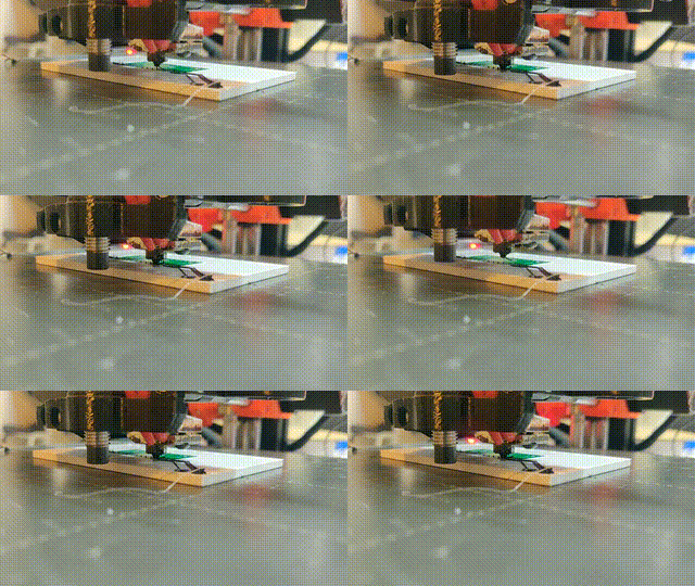
The main idea behind the process is to use tools that are already good at what they do for what they should be used for and efficiently bridge between those tools to create functional prototypes.
This project is in it's early stages, and as it develops the plan is to wrap many of the manual processes up with scripts, but still allow a user to easily access intermediary files in order to develop their own process flows for device prototyping
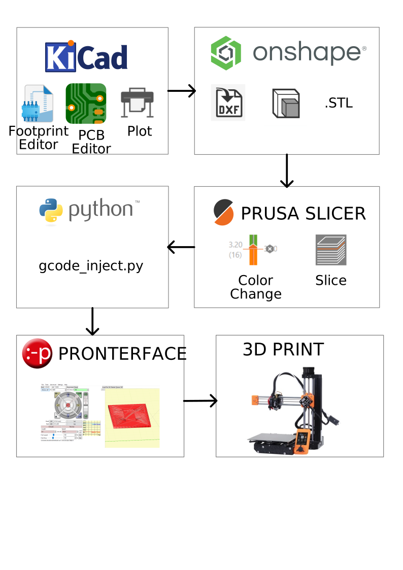
PCBs are designed in KiCad to then load them into a 3D modelling software, to then be sliced by a 3D Printer slicer, to finally have extra g-code added by a custom script that had the necessary information to inject conductive filament into the plated though holes of a PCB.
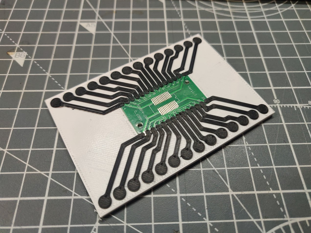
| Qty | Value | Footprint | References |
|---|---|---|---|
| 8 | Conn_01x20_Pin | Project:1x10 test pad | J2, J2, J3, J3, J4, J4, J5, J5 |
| 4 | Conn_01x20_Pin | Connector_PinHeader_2.54mm:PinHeader_1x10_P2.54mm_Vertical | J1, J1, J6, J6 |
It measures 25.4 × 50.8 mm and has 2 copper layers, 1.6 mm thick.
12 parts. The full list of its parts is on this page, with links to each part's symbol and footprint where PCBKit's library has them.
From the ollyoid/splic3r repository on GitHub, at the commit this page was made from: the board is demo_files/Characterisation Board/Characterisation Board.kicad_pcb and its schematic demo_files/Characterisation Board/Characterisation Board.kicad_sch. PCBKit opens the board in the browser, with nothing to install.
Its repository states no licence, so its author keeps all rights: ask ollyoid before reusing the design.
github-linguist/linguist
Language Savant. If your repository's language is being reported incorrectly, send us a pull request!


google/mozc-devices
Circuit diagrams and firmware source code for Gboard DIY keyboards


hackclub/OnBoard
💡 Join 1,000 teenagers and make your first PCB with a $100 grant!

VoronDesign/Voron-Tap
Tap is a nozzle-based z-probe for the V2 and Trident printer designs. The entire toolhead moves to trigger an optical switch. Tap offers many advantages:

stacksmashing/pico-tpmsniffer
A simple, very experimental TPM sniffer for LPC bus