
2 layers30.4 × 12.7 mm
 nulllaborg/CH5xxDuino3
base ch552 dap-nano
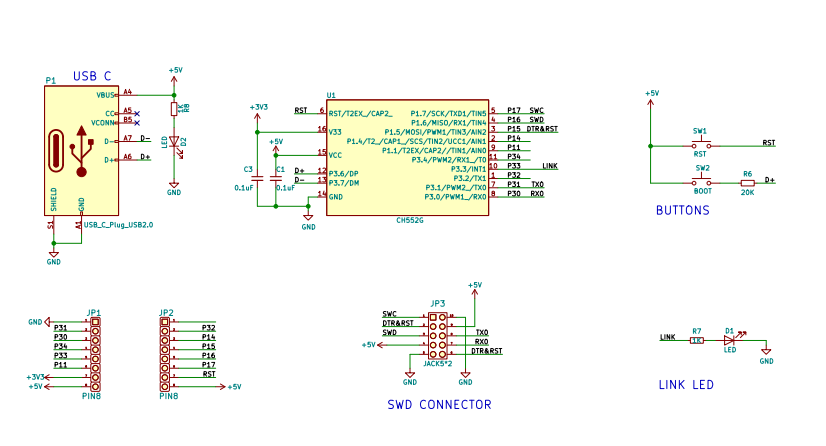
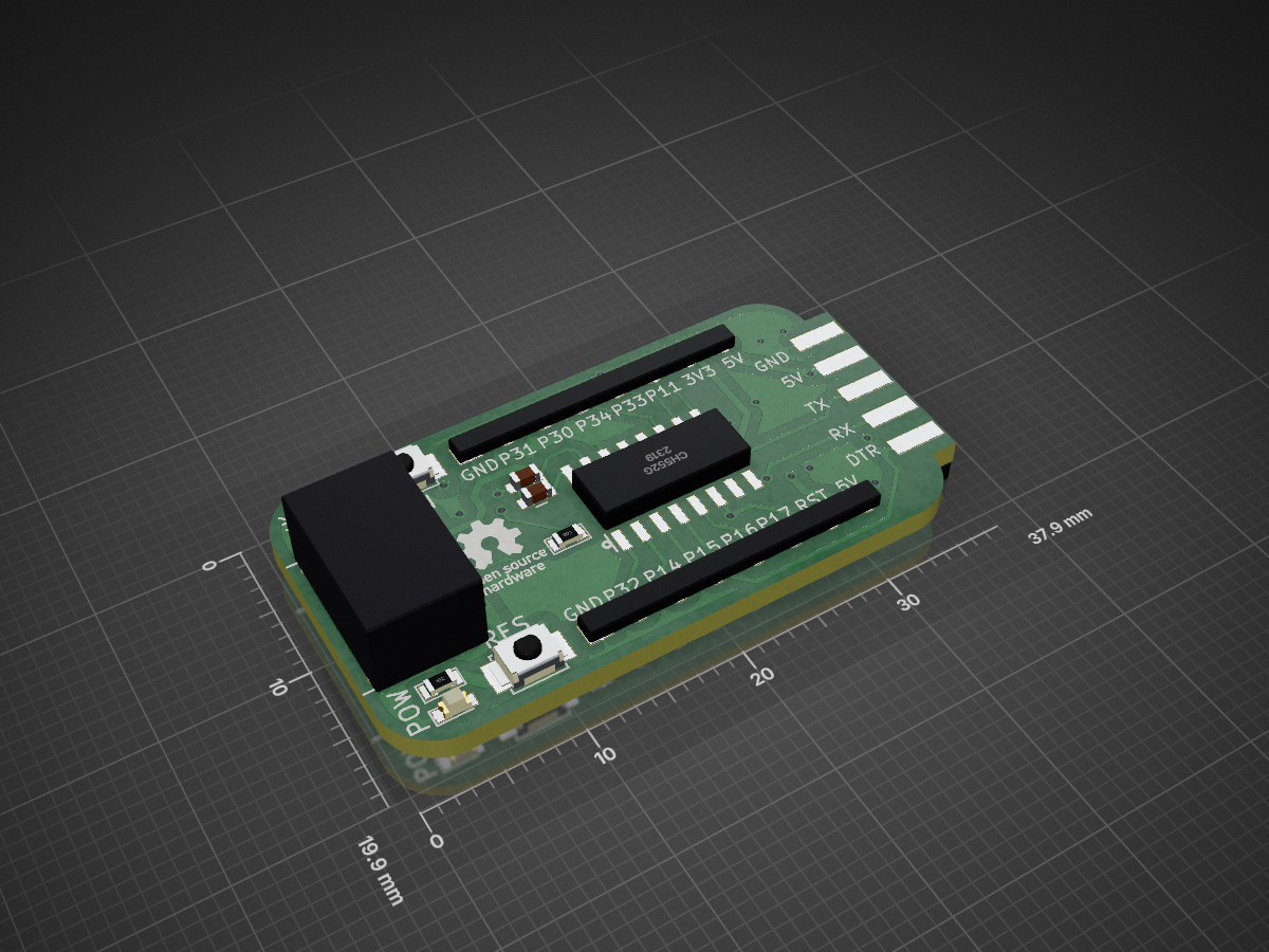
CH5xxDuino Nano is an open-source printed circuit board by nulllaborg, from the nulllaborg/CH5xxDuino repository on GitHub. It is a 2-layer board of 37.9 × 19.9 mm with 15 parts on 21 nets, routed with 235 tracks and 30 vias.
It is built around the CH552G. Its parts include 3 resistors, 2 capacitors, 2 diodes, 2 switches and 1 IC. It belongs with the 8051 (CH55x, STC, AT89) boards of this library.
| Qty | Value | Footprint | References |
|---|---|---|---|
| 2 | 0.1uF | ch5xxduino-nano:C_0603 | C1, e |
| 2 | 1K | ch5xxduino-nano:R_0603 | R7, R8 |
| 2 | LED | ch5xxduino-nano:LED_0603 | D1, D2 |
| 2 | PIN8 | ch5xxduino-nano:DIP-1.5Hole-2.54mm-Pitch-8P | JP1, JP2 |
| 1 | 20K | ch5xxduino-nano:R_0603 | R6 |
| 1 | BOOT | ch5xxduino-nano:SW_SPST_B3U-1000P | SW2 |
| 1 | CH552G | CH5xxDuino-Nano:SOIC-16_3.9x9.9mm_Pitch1.27mm | U1 |
| 1 | JACK5*2 | CH5xxDuino-Nano:SMD_CONN_5P | JP3 |
| 1 | LOGO | CH5xxDuino-Nano:open-hardware | G*** |
| 1 | RST | ch5xxduino-nano:SW_SPST_B3U-1000P | SW1 |
| 1 | USB_C_Plug_USB2.0 | ch5xxduino-nano:C393939 | P1 |
It measures 37.9 × 19.9 mm and has 2 copper layers, 1.6 mm thick.
15 parts, built around the CH552G. The full list of its parts is on this page, with links to each part's symbol and footprint where PCBKit's library has them.
From the nulllaborg/CH5xxDuino repository on GitHub, at the commit this page was made from: the board is hardware/CH5xxDuino-Nano.kicad_pcb. PCBKit opens the board in the browser, with nothing to install.
Its repository states no licence, so its author keeps all rights: ask nulllaborg before reusing the design.


milar111/L.I.P.S.
OpenSource Affordable SipAndPuff device: Linear Interface for Paralysis Support


gowenrw/BSidesDFW_2019_Badge
This is where all the files for the BSidesDFW 2019 Badge will be stored. This includes code and art and cab and fab files. All the things.
