2 layers70.1 × 47.1 mm

 nrivard/n8-Bit10
65C02 Microcomputer
N8 bit special is an open-source printed circuit board by nrivard, from the nrivard/n8-Bit repository on GitHub, published under the MIT licence. It is a 4-layer board of 99.9 × 100 mm with 50 parts on 108 nets, routed with 1,486 tracks and 18 vias.
It is built around the CH340C, 74HC00D and 74LS21PC, with the DS1813-5+ among its other parts. Its parts include 18 capacitors, 10 ICs, 5 resistors, 5 connectors and 3 diodes.


The n8 Bit Microcomputer is a homebrew breadboard computer built around a WDC65C02 8-bit CPU. If you are looking for the software that runs on this computer, check out LmaOS.
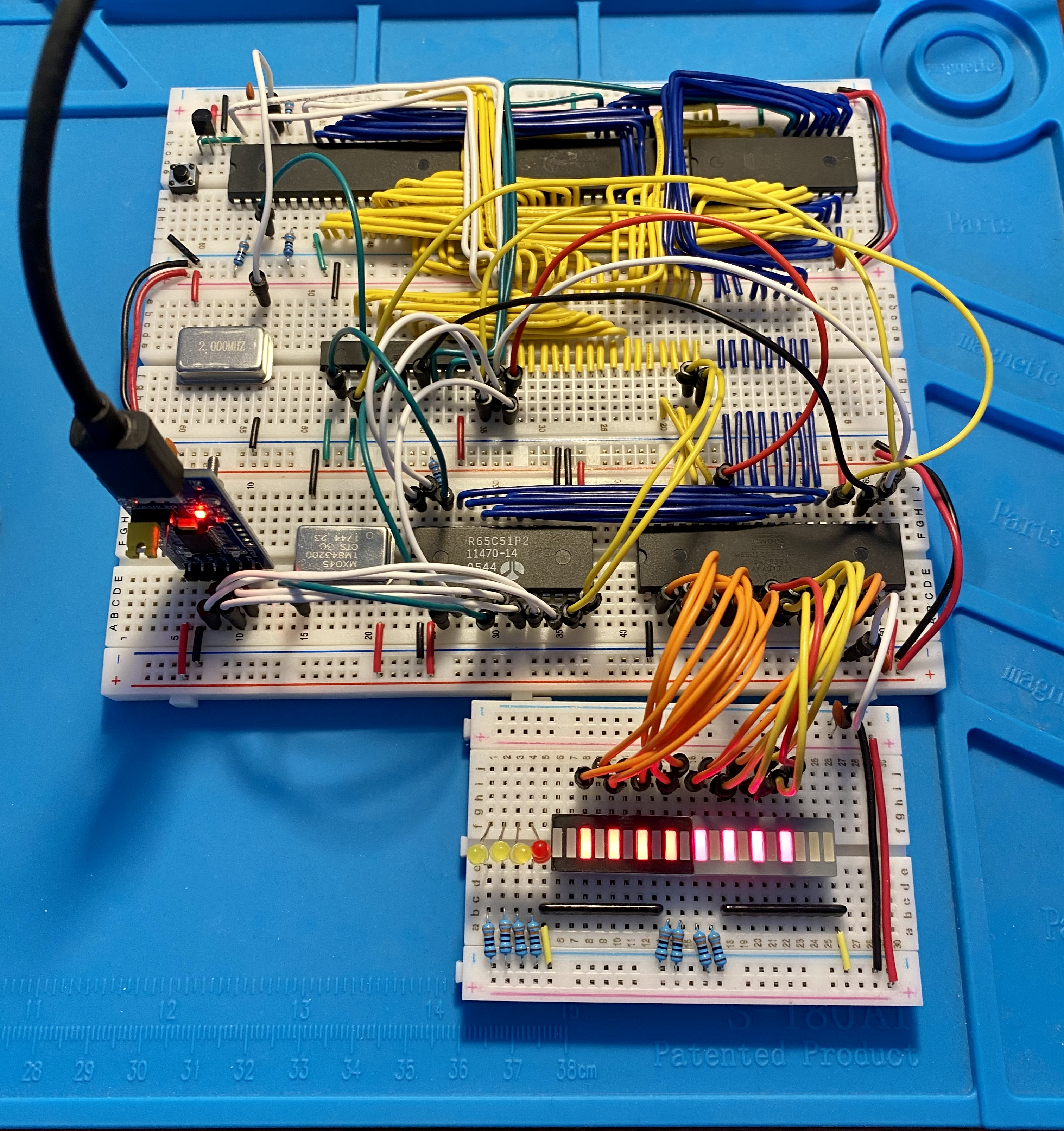
The n8 Bit was originally a breadboard computer based on the Ben Eater series of 6502 videos but with some added capabilities including ACIA support, GAL-based address decoding logic, and a power chip for more reliable reset and power-on. Since then, PCBs have been printed and development around the computer is based on these.
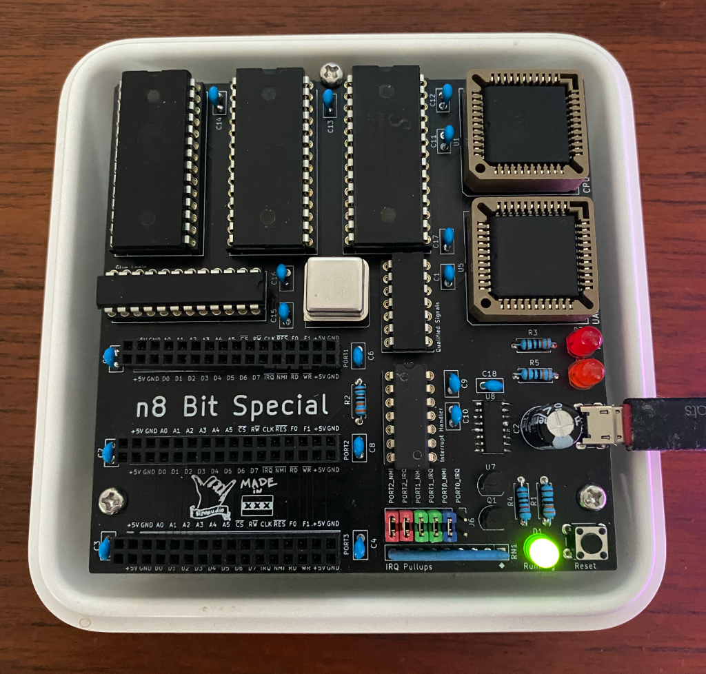
Large PCBs are expensive and I am not a rich person. For this reason, the main goal of the physical design of this computer and the expansion cards is to fit on the $5 boards at the cheap PCB houses. This gives a maximum area of 100mm x 100mm, which this board attempts to utilize to the utmost.
The v2 main board is built around a WDC65C02 CPU operating at 3.6864Mhz and is meant to be as minimally viable as possible. It consists of:
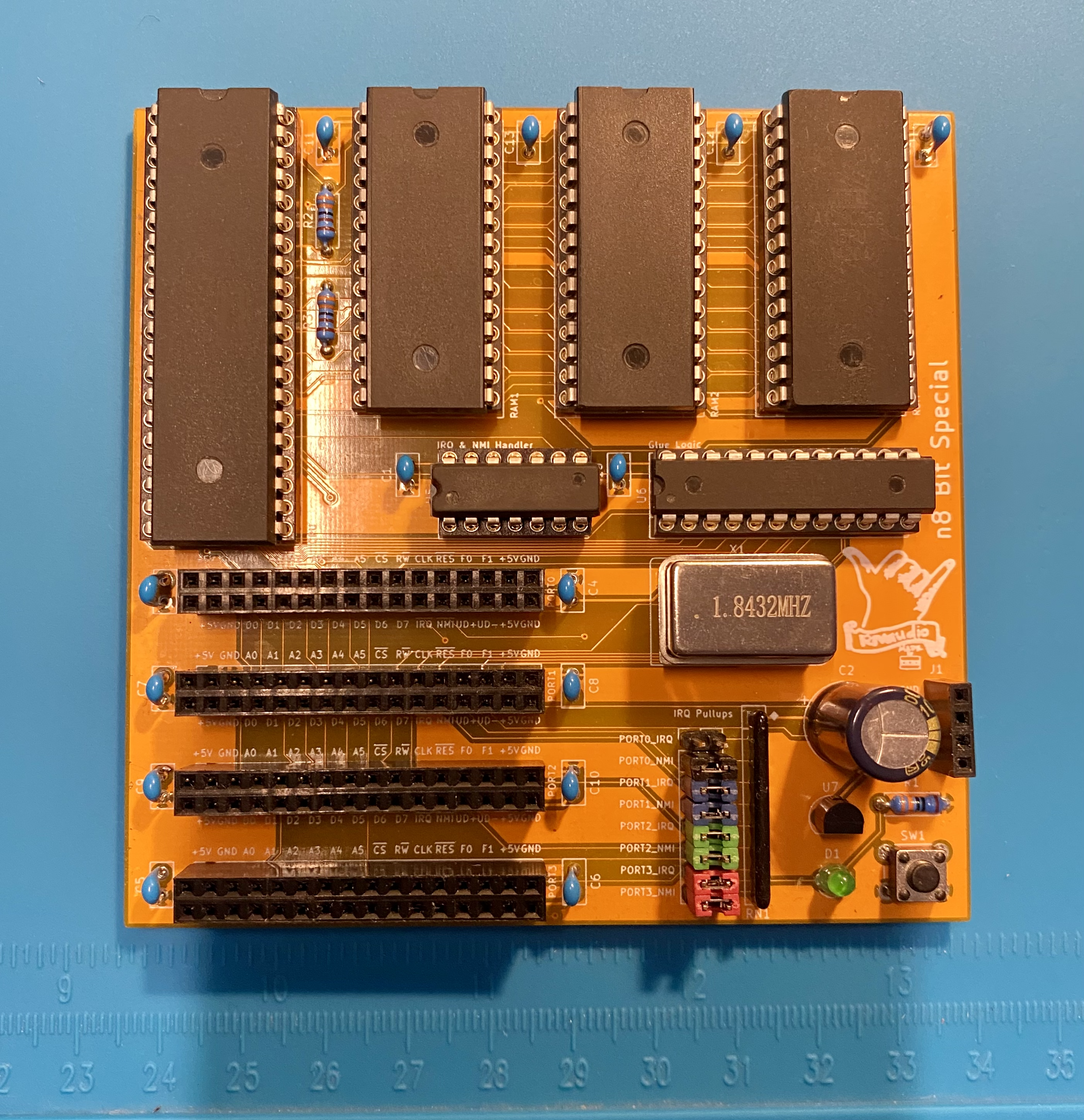
By default, the n8 Bit is intended to have the following memory hardware:
If you are using the default hardware and the included GAL code, it has the following memory layout:
| Device | Address Range |
|---|---|
| Zero Page | $0000...$00FF |
| Stack | $0100...$01FF |
| RAM | $0200...$BEFF |
| Port 0 | $BF00...$BF3F |
| Port 1 | $BF40...$BF7F |
| Port 2 | $BF80...$BFBF |
| DUART | $BFC0...$BFFF |
| ROM | $C000...$FFFF |
This configuration has 16K of ROM, 48k (less one page) of RAM, and 1 page of memory ($BF00...$BFFF) dedicated to 3 I/O ports and the DUART, each of which has 64 addressable memory locations.
Because address decoding is entirely GAL based, you have a lot of room to customize the address space. The GAL itself has physical connections to each port and to each memory socket for CS signals. How you utilize these (or even if you utilize them) is entirely up to you. If you wanted a simpler computer (like the Ben Eater computer) you may opt to leave one memory socket open and only use a single RAM and a single ROM chip. If you go this route, you will have to update your own GAL code to match your hardware configuration.
The biggest advancement with the n8 Bit when it moved from breadboards to custom PCBs is the introduction of the n8 Bus spec.
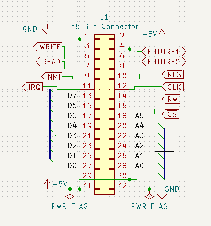
The spec mandates that the following signals will be available on a standard 2x16 board-to-board female header:
Bidirectional signals:
Read-only signals:
Write-only signals:
Expansion signals:
The n8 Bus spec includes 2 lines (FUTURE0 and FUTURE1) that don't currently have a purpose.
These are hooked up to 2 I/O pins of the GAL and are intended for you to customize them.
For example, if you have a VDP that outputs a colorburst clock that you want to use to drive a sound adapter, you can route that signal through one of these pins.
Power Rails:
The n8 Bus spec provides power rails (+5V and ground) on both the top and bottom of the header for shorter, more convenient power routing on your expansions cards.
The main board for this computer is intentionally minimal. This means that all of your I/O functionality beyond a DUART (VIA, display, sound, etc.) has to come in the form of an expansion card that sits in a n8 Bus port.
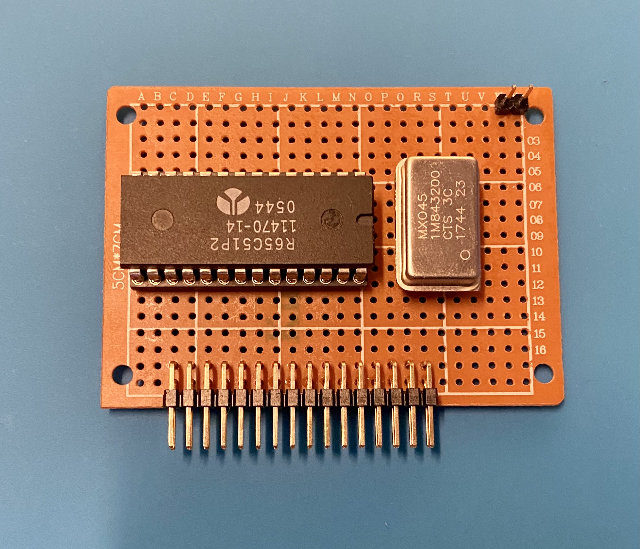
Two highly utilized devices that many hobbyists want to include on a homebrew computer are a UART (this is unnecessary now on the v2 board but is kept for reference purposes) and a GPIO device. In this repo, 2 such reference designs are included:
If you want to create your own cards, it's best to copy one of the existing reference designs first. This is because they will already have:
This will ensure you have consistent and correct card designs from the start.
NMI and IRQ are supported for all 3 n8 Bus ports. This board uses a WDC65C02 which uses a totem-pole design (the NMOS 6502 used an open-drain design) and so the board also includes optional jumpers for pull-up resistors. In general:
See this article from Garth Wilson for more information.
There are no known hardware bugs with the v2 board. If you find one (or more) please raise an issue.
| Qty | Value | Footprint | References |
|---|---|---|---|
| 13 | 100nf | Capacitor_THT:C_Disc_D5.0mm_W2.5mm_P2.50mm | C1, C3, C4, C5, C6, C7, C8, C11, C12, C13, C14, C15, C16 |
| 4 | 100nF | Capacitor_THT:C_Disc_D5.0mm_W2.5mm_P2.50mm | C9, C10, C17, C18 |
| 3 | 220 | Resistor_THT:R_Axial_DIN0207_L6.3mm_D2.5mm_P7.62mm_Horizontal | R1, R3, R5 |
| 3 | LED_ALT | LED_THT:LED_D3.0mm | D1, D2, D3 |
| 2 | CY62256-70PC | Package_DIP:DIP-28_W15.24mm_Socket | U2, U3 |
| 1 | 10K | Resistor_THT:R_Axial_DIN0207_L6.3mm_D2.5mm_P7.62mm_Horizontal | R4 |
| 1 | 22V10C | Package_DIP:DIP-24_W7.62mm_Socket | U6 |
| 1 | 28C256 | Package_DIP:DIP-28_W15.24mm_Socket | U4 |
| 1 | 2N3904 | Package_TO_SOT_THT:TO-92 | Q1 |
| 1 | 3.6864Mhz | Oscillator:Oscillator_DIP-8 | X1 |
| 1 | 3K3 | Resistor_THT:R_Axial_DIN0207_L6.3mm_D2.5mm_P7.62mm_Horizontal | R2 |
| 1 | 3K3 | Resistor_THT:R_Array_SIP9 | RN1 |
| 1 | 470uF | Capacitor_THT:CP_Radial_D8.0mm_P3.80mm | C2 |
| 1 | 74HC00 | Package_DIP:DIP-14_W7.62mm_Socket | U10 |
| 1 | 74LS21 | Package_DIP:DIP-14_W7.62mm_Socket | U9 |
| 1 | CH340C | Package_SO:SOIC-16_3.9x9.9mm_P1.27mm | U8 |
| 1 | Conn_02x08_Odd_Even | Connector_PinHeader_2.54mm:PinHeader_2x06_P2.54mm_Vertical | J6 |
| 1 | DS1813 | Package_TO_SOT_THT:TO-92 | U7 |
| 1 | LOGO | graphics:MadeInAMS | G2 |
| 1 | LOGO | graphics:Shaka | G1 |
| 1 | PORT0 | Connector_PinSocket_2.54mm:PinSocket_2x16_P2.54mm_Vertical | J2 |
| 1 | PORT1 | Connector_PinSocket_2.54mm:PinSocket_2x16_P2.54mm_Vertical | J3 |
| 1 | PORT2 | Connector_PinSocket_2.54mm:PinSocket_2x16_P2.54mm_Vertical | J4 |
| 1 | SC28L92_PLC44 | Package_LCC:PLCC-44_THT-Socket | U5 |
| 1 | SW_Push_Dual | Button_Switch_THT:SW_PUSH_6mm | SW1 |
| 1 | USB_B_Micro | Connector_USB:USB_Micro-B_Wuerth_629105150521 | J1 |
| 1 | W65C02SxP | Package_LCC:PLCC-44_THT-Socket | U1 |
The 47 most common of 50 parts.


Trilobyte-CPU/8-bit-computer
A DIY 8-bit computer built mostly with discrete logic chips

snippyrow/-816-board
A retro computer motherboard for the W65C816S CPU. Dual-core expandable, 16mb extended memory, four expansion ports.


It measures 99.9 × 100 mm and has 4 copper layers, 1.6 mm thick.
50 parts, built around the CH340C, 74HC00D, 74LS21PC and DS1813-5+. The full list of its parts is on this page, with links to each part's symbol and footprint where PCBKit's library has them.
From the nrivard/n8-Bit repository on GitHub, at the commit this page was made from: the board is PCB/n8 bit special/n8 bit special.kicad_pcb and its schematic PCB/bouncer/bouncer.kicad_sch. PCBKit opens the board in the browser, with nothing to install.
Its repository publishes it under the MIT licence: you may reuse it on that licence's terms (keep the author's notice, and for a copyleft licence share your changes alike).