2 layers103 × 30.5 mm
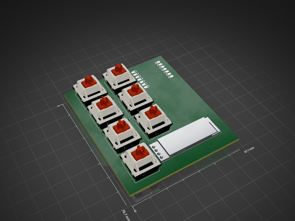
 nouxinf/hackpad
This is my submission for the hackpad mission! This is my first time using KiCad and Autodesk Fusion so I'm not very experienced.
Hackpad is an open-source printed circuit board by nouxinf, from the nouxinf/hackpad repository on GitHub, published under the MIT licence. It is a 2-layer board of 67.1 × 78.7 mm with 9 parts on 14 nets, routed with 97 tracks and 32 vias.
Its parts include 7 switches, 1 IC and 1 connector.
This is my submission for the hackpad mission! This is my first time using KiCad and Autodesk Fusion so I'm not very experienced. Decided to make this because I wanted to make some automation easier, as it binds the keys to F13-19, which are unused usually.
It also includes a bongo cat animation, that activates when you press any key on the macropad. Code is from github over here.
| Name | Quantity |
|---|---|
| Seeed XIAO RP2040 microcontroller | 1 |
| MX-style mechanical switches | 7 |
| 0.91" 128x32 OLED Display | 1 |
| Blank DSA keycaps | 7 |
| M3x16mm Screws | 4 |
| M3x5x4mm heatset inserts | 4 |
| PCB | 1 |
| Case | 1 |
Also available in bom.csv
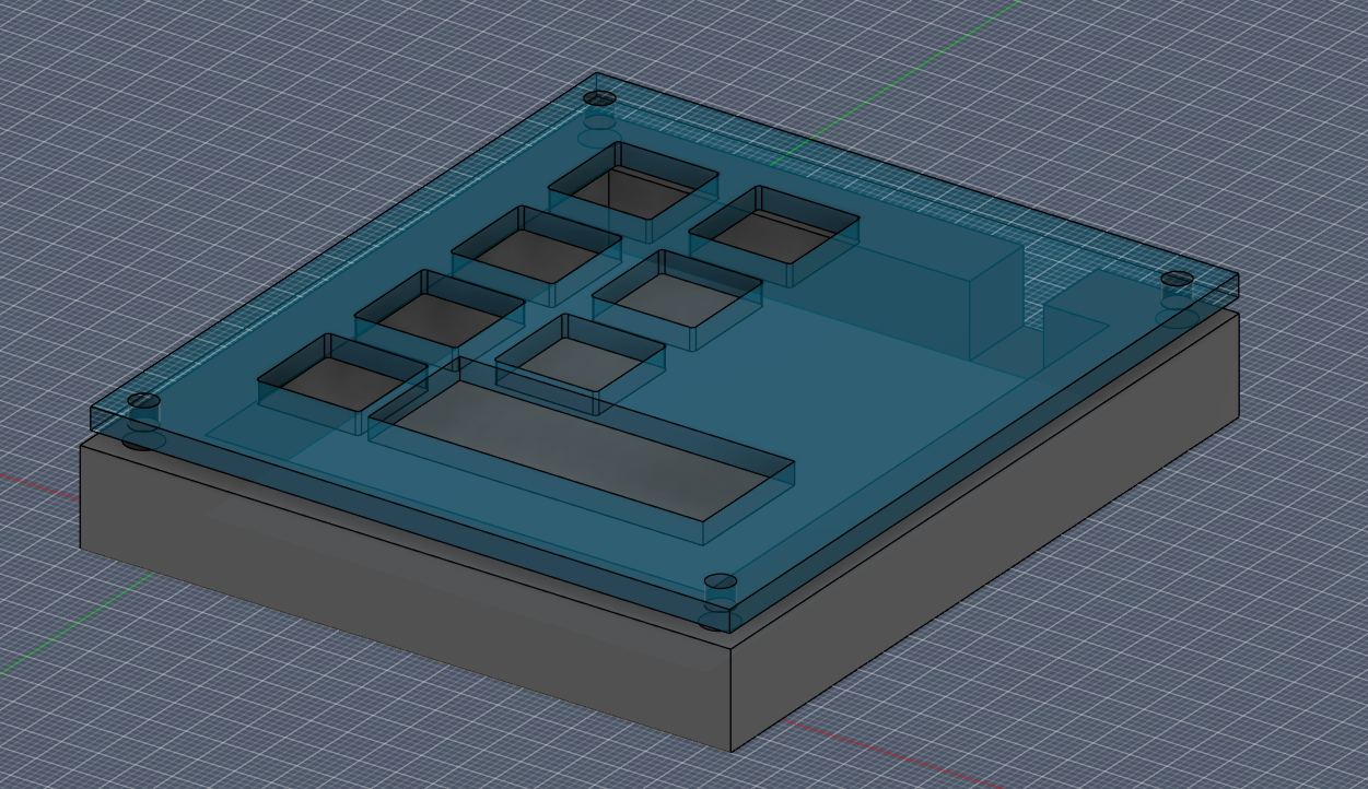 The case assembled (top part made transparent for visibility, not in actual model)
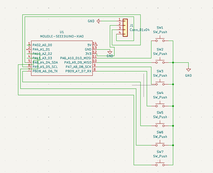 Schematic of the PCB
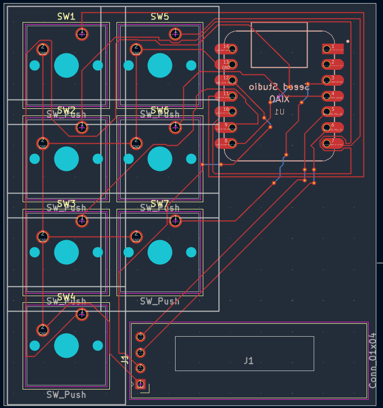 PCB design
| Qty | Value | Footprint | References |
|---|---|---|---|
| 7 | SW_Push | Button_Switch_Keyboard:SW_Cherry_MX_1.00u_PCB | SW1, SW2, SW3, SW4, SW5, SW6, SW7 |
| 1 | Conn_01x04 | Display:ER_OLEDM0.91_1x-I2C | J1 |
| 1 | MOUDLE-SEEEDUINO-XIAO | footprints:XIAO-Generic-Hybrid-14P-2.54-21X17.8MM | U1 |
It measures 67.1 × 78.7 mm and has 2 copper layers, 1.6 mm thick.
9 parts. The full list of its parts is on this page, with links to each part's symbol and footprint where PCBKit's library has them.
From the nouxinf/hackpad repository on GitHub, at the commit this page was made from: the board is PCB/hackpad.kicad_pcb and its schematic PCB/hackpad.kicad_sch. PCBKit opens the board in the browser, with nothing to install.
Its repository publishes it under the MIT licence: you may reuse it on that licence's terms (keep the author's notice, and for a copyleft licence share your changes alike).


FrameworkComputer/ExpansionCards
Reference designs and documentation to create Expansion Cards for the Framework Laptop

VoronDesign/Voron-Hardware
Cool Hardware designed by the Voron Design group

hackclub/OnBoard
💡 Join 1,000 teenagers and make your first PCB with a $100 grant!


adamws/kicad-kbplacer
KiCad plugin for automatic keyboard's key placement and routing