2 layers52.3 × 10.5 mm
StackLink
gusmanb/logicanalyzer
24 channel, 100Msps logic analyzer hardware and software
29 parts5.1kGPL-3.0

 Neumi/wifi_camera25
A camera that can see WiFi signals.
Wifi camera is an open-source printed circuit board by Neumi, from the Neumi/wifi_camera repository on GitHub. It is a 2-layer board of 99 × 99 mm with 29 parts on 38 nets, routed with 527 tracks and 14 vias.
Its parts include 16 ICs, 4 resistors, 3 connectors, 1 capacitor and 1 switch. It belongs with the radio and wireless boards and the ESP8266 boards of this library.
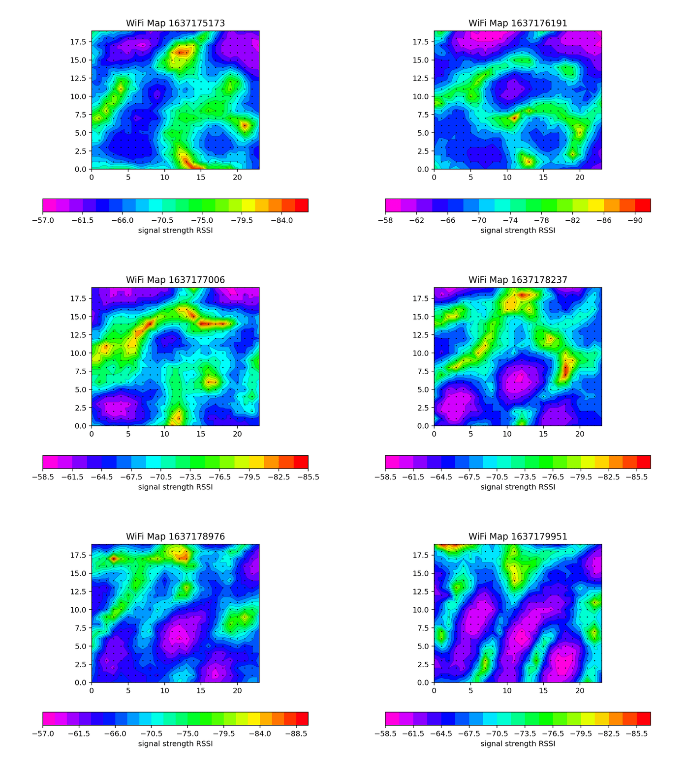 3D capture of a wifi signal in a 20x20x20 cm grid.
The sensor array captures RSSI values from near by WiFi networks and sends the collected pixel data to a master that processes and visualizes the captured data. The goal is to build a sensor, that makes WiFi signal visible in more or less real time.
WiFi signals are invisible to humans. I think it would be fun to make them visible and play around with it. Projects I have in mind unsing the sensor array: real time analysis of antennas and obstacles..., real time object/person detection/tracking by reading WiFi shadows and reflections, using the standing wave to 'surf' it to get position data back for i.e. robots.
Before this, I built a rig to scan and visualize WiFi signal propagation in 3D
https://hackaday.com/2021/11/22/visualizing-wifi-with-a-converted-3d-printer/
https://github.com/Neumi/3D_wifi_scanner
This got me interested in building a real time, sensor array to take a whole frame at once without having to scan a slice one position after another.
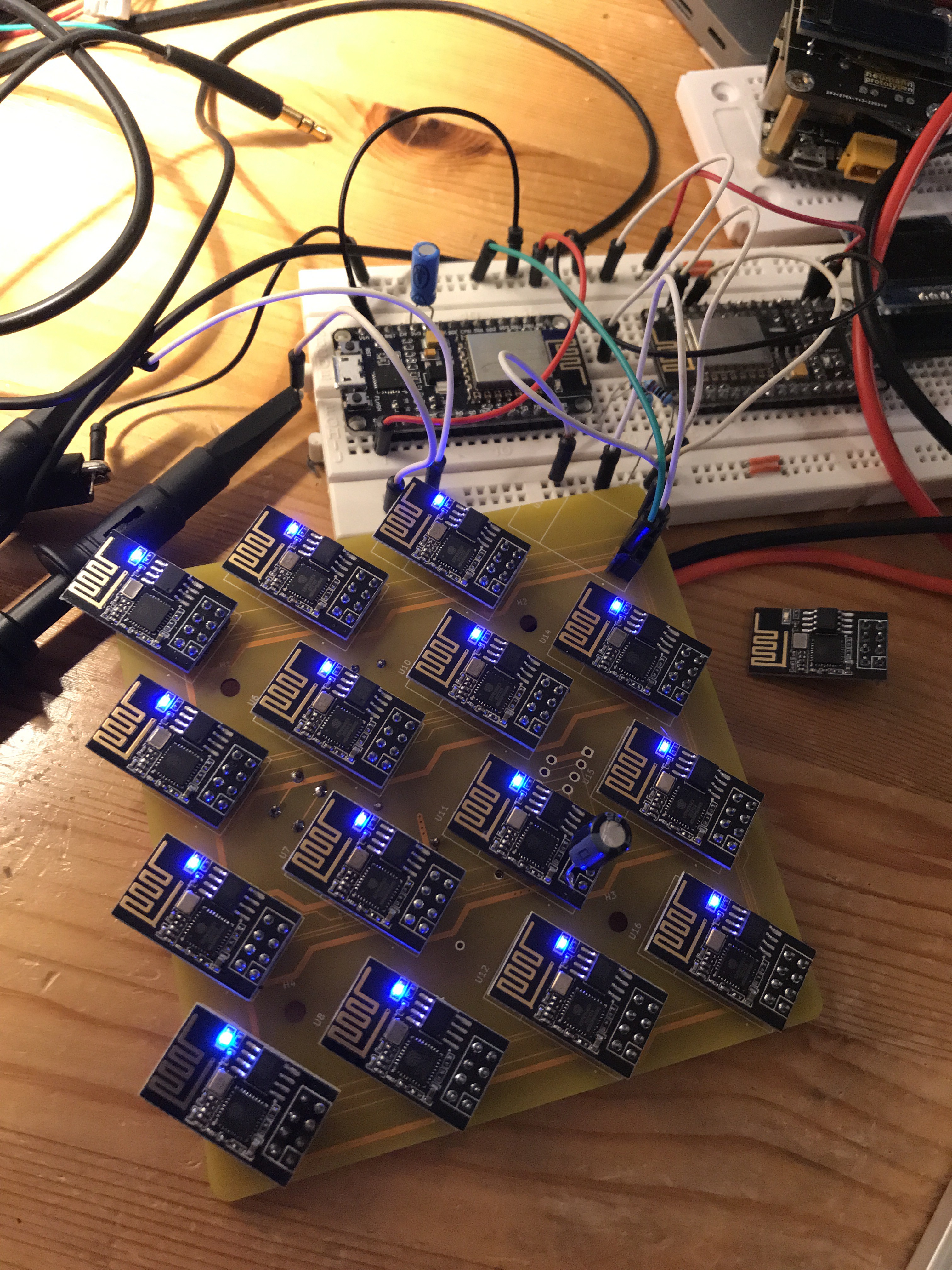
To capture a whole slice at once, I built this array unsing four PCBs with 4x4 ESP8266 sensor nodes connected via i2c where every pixel is an i2c slave and a master that asks the pixels one by one for the captured values.
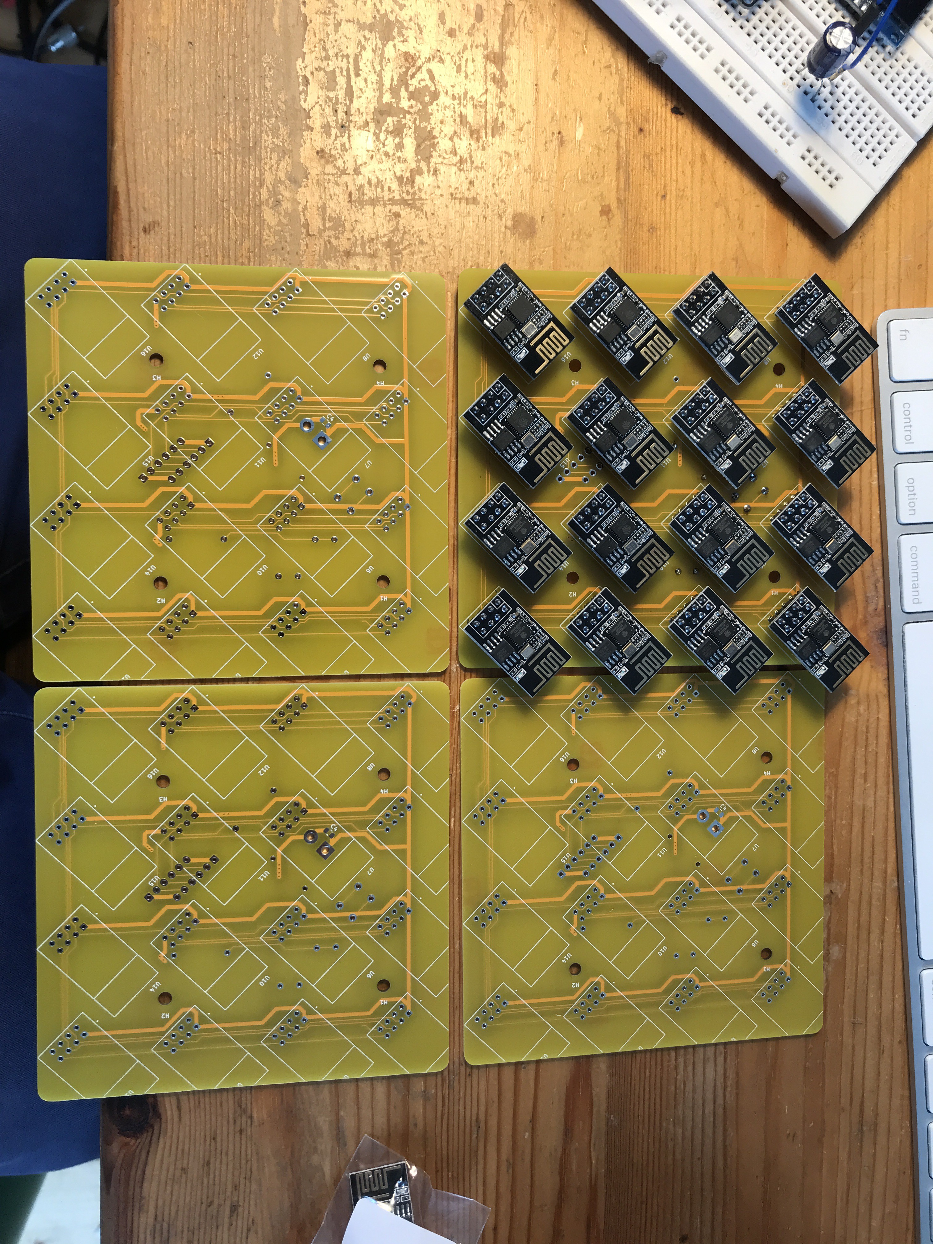
I'm currently waiting fore more ESP8266s to arrive.
The results look pretty granular currently, as I only used 4x4 pixels, which is a bit low. When more ESPs arrive, I will take more images.
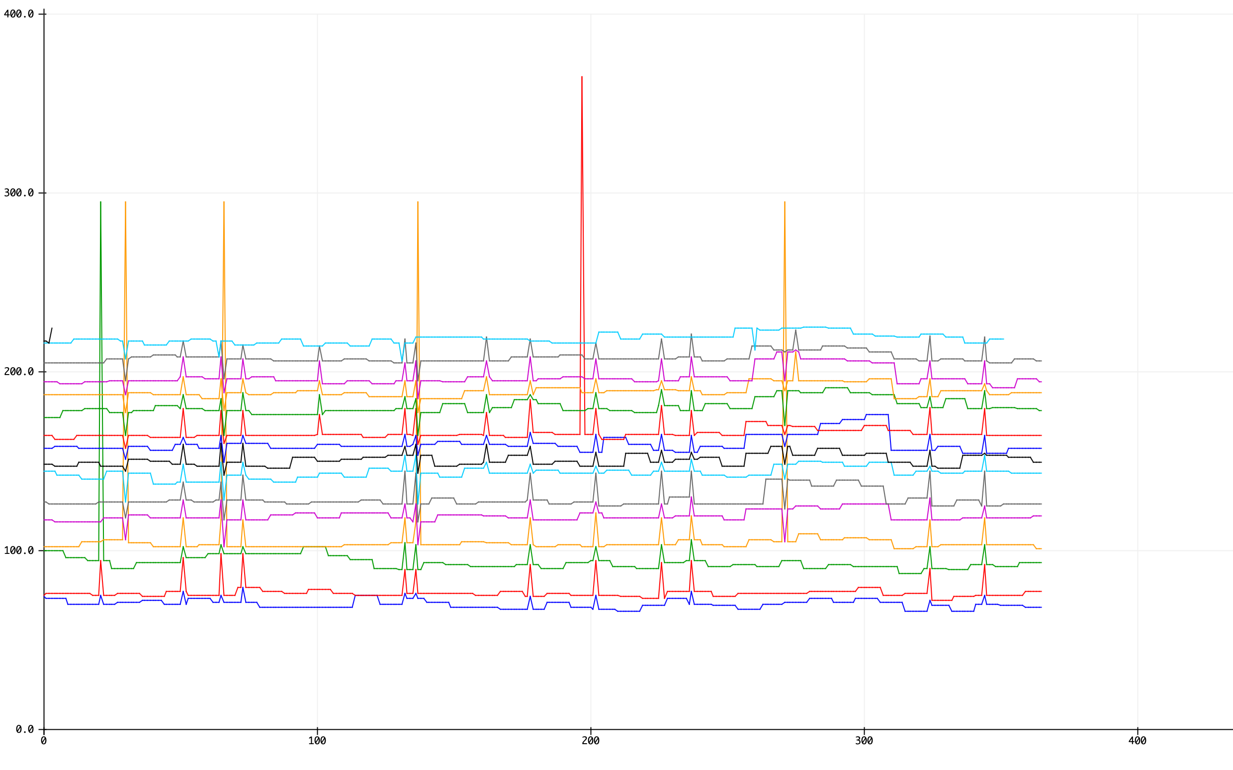 16 Pixels, x-axis is time, Y axis is RSSI with an offset between each pixel for visibility.
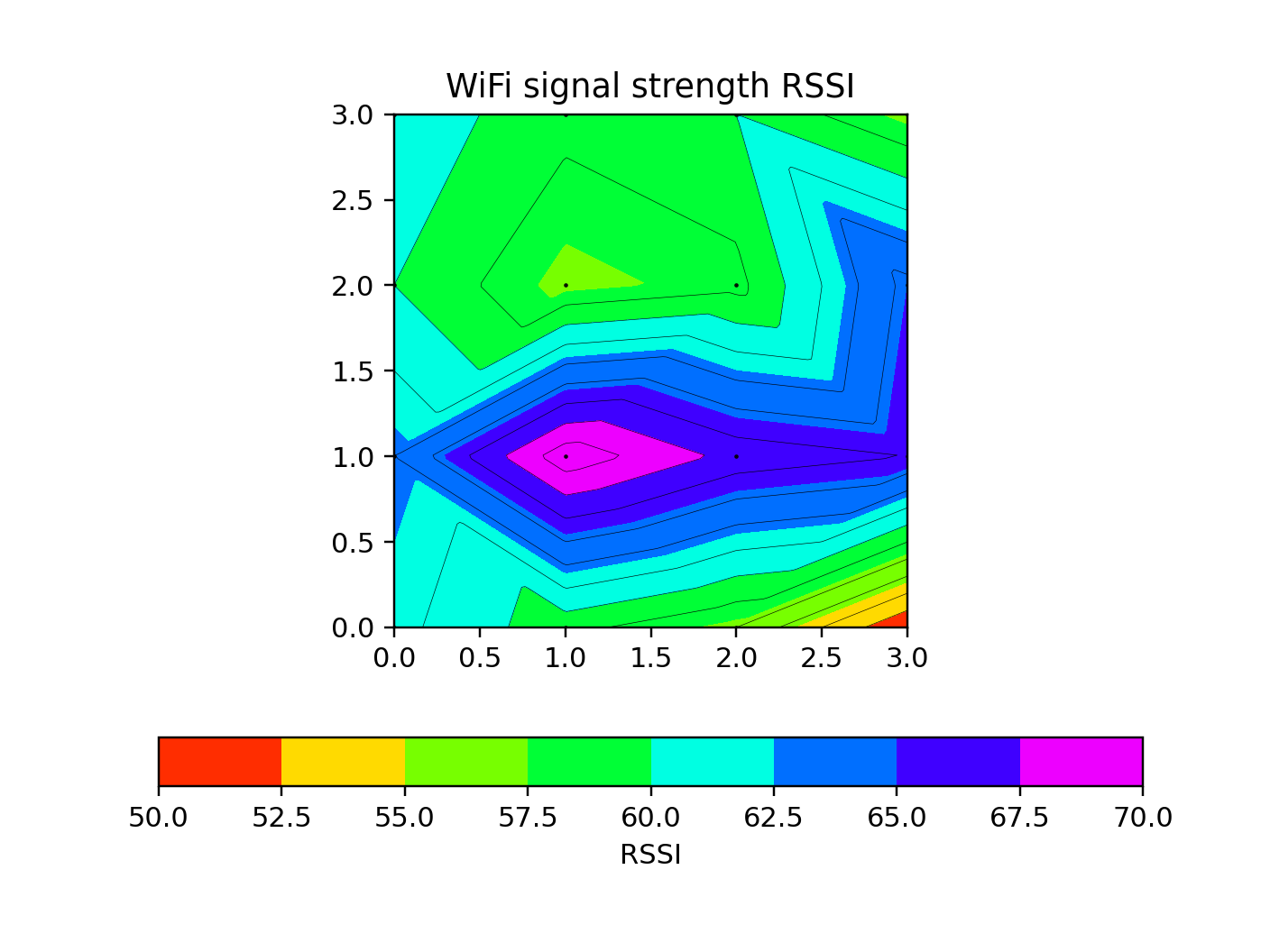 16 Pixels with correct orientation in a 2D plot.

| Qty | Value | Footprint | References |
|---|---|---|---|
| 16 | ESP8266-01_ESP-01 | KiCad:XCVR_ESP8266-01_ESP-01 | U1, U2, U3, U4, U5, U6, U7, U8, U9, U10, U11, U12, U13, U14, U15, U16 |
| 4 | MountingHole | MountingHole:MountingHole_3.2mm_M3 | H1, H2, H3, H4 |
| 3 | 4k7 | Resistor_THT:R_Axial_DIN0309_L9.0mm_D3.2mm_P12.70mm_Horizontal | R2, R3, R4 |
| 2 | Conn_01x06_Male | Connector_JST:JST_EH_B6B-EH-A_1x06_P2.50mm_Vertical | J2, J3 |
| 1 | 100nF | Capacitor_SMD:C_0805_2012Metric | C4 |
| 1 | 1k | Resistor_THT:R_Axial_DIN0309_L9.0mm_D3.2mm_P12.70mm_Horizontal | R1 |
| 1 | Conn_01x02_Male | Connector_AMASS:AMASS_XT30PW-M_1x02_P2.50mm_Horizontal | J1 |
| 1 | SW_Push | Button_Switch_THT:SW_PUSH_6mm | SW1 |
It measures 99 × 99 mm and has 2 copper layers, 1.6 mm thick.
29 parts. The full list of its parts is on this page, with links to each part's symbol and footprint where PCBKit's library has them.
From the Neumi/wifi_camera repository on GitHub, at the commit this page was made from: the board is electronics/wifi_camera.kicad_pcb and its schematic electronics/wifi_camera.kicad_sch. PCBKit opens the board in the browser, with nothing to install.
Its repository states no licence, so its author keeps all rights: ask Neumi before reusing the design.
gusmanb/logicanalyzer
24 channel, 100Msps logic analyzer hardware and software

VoronDesign/Voron-Hardware
Cool Hardware designed by the Voron Design group

hoglet67/RGBtoHDMI
Bare-metal Raspberry Pi project that provides pixel-perfect sampling of Retro Computer RGB/YUV video and conversion to HDMI

hackclub/OnBoard
💡 Join 1,000 teenagers and make your first PCB with a $100 grant!

OLIMEX/DIY-LAPTOP
Do It Yourself Open Source Hardware and Software Modular Hacker's Friendly Laptop

UtilitechAS/amsreader-firmware
ESP8266 and ESP32 compatible firmware to read, interpret and publish data to MQTT from smart electrical meters, both DLMS and DSMR is supported

