
4 layers71.9 × 94 mm
Thumbdeck left
neuman/gripster
thumbdeck — wireless split thumb keyboard (nRF52840 + ZMK, BLE split, i8+-inspired). Layout converged & graded PASS.
87 parts11Apache-2.0

 neuman/gripster11
thumbdeck — wireless split thumb keyboard (nRF52840 + ZMK, BLE split, i8+-inspired). Layout converged & graded PASS.
Thumbdeck right is an open-source printed circuit board by neuman, from the neuman/gripster repository on GitHub, published under the Apache-2.0 licence. It is a 4-layer board of 71.9 × 94 mm with 114 parts on 74 nets, routed with 1,743 tracks and 262 vias.
It is built around the E73-2G4M08S1C, MCP73831 and USBLC6-2SC6, with the 1N4148WS, MSK12C02 and TS-1187A-B-A-B among its other parts. Its parts include 38 switches, 37 diodes, 17 resistors, 8 capacitors and 4 ICs. It belongs with the keyboards and input and radio and wireless boards of this library.


A wireless thumb keyboard that turns your phone into a handheld deck. The phone clamps landscape in the middle on a spring-loaded expanding bridge (Kishi/Backbone style, 130–170 mm phones); two grips flank it, and you thumb-type a 78-key QWERTY on metal snap domes over Bluetooth.
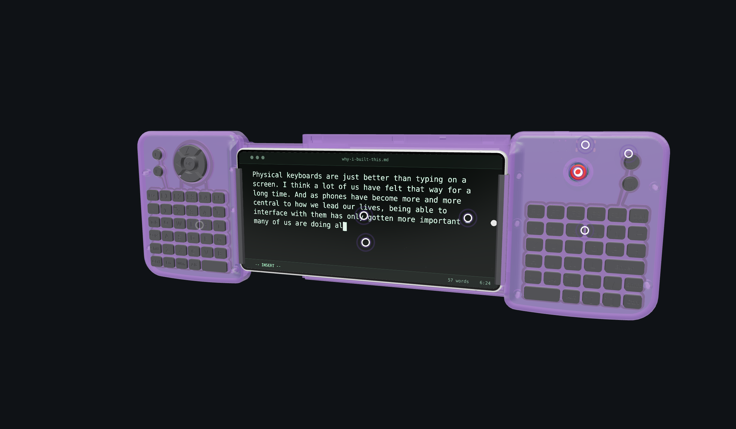
Click the image to spin the assembly in 3D, pull it apart, and slide the clamp through its travel.


The phone sits down inside a well so the glass and the keyboard face form one flat plane 14.7 mm off the back. Two contoured grips flank it, GBC-styled: boxy outline, translucent Atomic-Purple shell, dark-gray keymats.
Despite the two halves, this is not a split keyboard. One nRF52840 module in the right grip scans a single 9×10 matrix; the left grip has no active silicon. A single 20-way FFC ribbon crosses the spine carrying both the matrix and the battery, so there is one BLE device, one battery and one firmware image.
  LEFT grip (passive)                        RIGHT grip (MCU)
  42 domes + diodes  ── 20-way FFC jumper ──  Ebyte E73 (nRF52840)  ⇄ phone (BLE HID)
  D-pad/OK, mouse       14 matrix + VBAT      + charger + USB-C + power switch
  LiPo + J4 + F1 PTC    + GND, one cable      scans the whole 9×10 matrix
There are no switches and no hand-soldering: 78 Snaptron 7 mm snap domes press directly onto gold ENIG pads, and everything soldered is SMT on one side of each board, so JLCPCB builds it turnkey.
Everything in this repo — the KiCad boards, the printable shells, the renders, the ZMK keymap — is
generated from one parametric Python file, hardware/scripts/deck.py.
Move a key and the pad, the shell opening, the keycap and the firmware matrix all move with it.
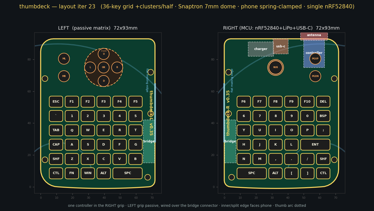
Naming: the project is Gripster, but every internal identifier — the ZMK board id, the board and
firmware filenames, the Bluetooth device name — is thumbdeck. Those are real strings in real
files.
| Keys | 78 Snaptron 7 mm snap domes (36 right / 42 left), rectangular 8.5 × 7 mm caps at 10 × 9 mm pitch, one-piece living-hinge TPU keymat with 2u space and 2u Enter |
| Clusters | Left: Ø24 integrated D-pad + mouse L/R. Right: hall-effect pointing nub (TrackPoint-style, rate control) + PgUp/PgDn |
| Modifiers | Mirrored on both grips (a thumb can't cross the phone gap); no sticky keys, all chords are plain holds |
| Controller | One Ebyte E73-2G4M08S1C (nRF52840 module, JLC C356849) |
| Matrix | Single 9×10, col2row, one 1N4148WS per key, 9× 4.7 kΩ row pull-downs |
| Bridge | 20-pin 1.0 mm FFC ZIF each side + a 20-way type-A jumper ≥240 mm |
| Boards | 75.0 × 97.0 mm each, 4-layer, 1.6 mm FR-4, ENIG (mandatory for dome contacts) |
| Power | 403040 LiPo (~450–500 mAh) with integrated PCM in the left grip, MCP73831 charger, USB-C, USBLC6-2 ESD, slide switch, F1 PPTC fuse on the cell side of the ribbon |
| Shell | 7 prints (PETG) + 2 TPU grippers; every part fits a 220 × 220 mm bed |
| Firmware | ZMK v0.3.0, real unibody board definition (not a split, not a shield) |
| Cost | Roughly $150–250 for 5 sets, boards + assembly only. Excludes domes, cell, ribbon, filament, hardware, probe, shipping |
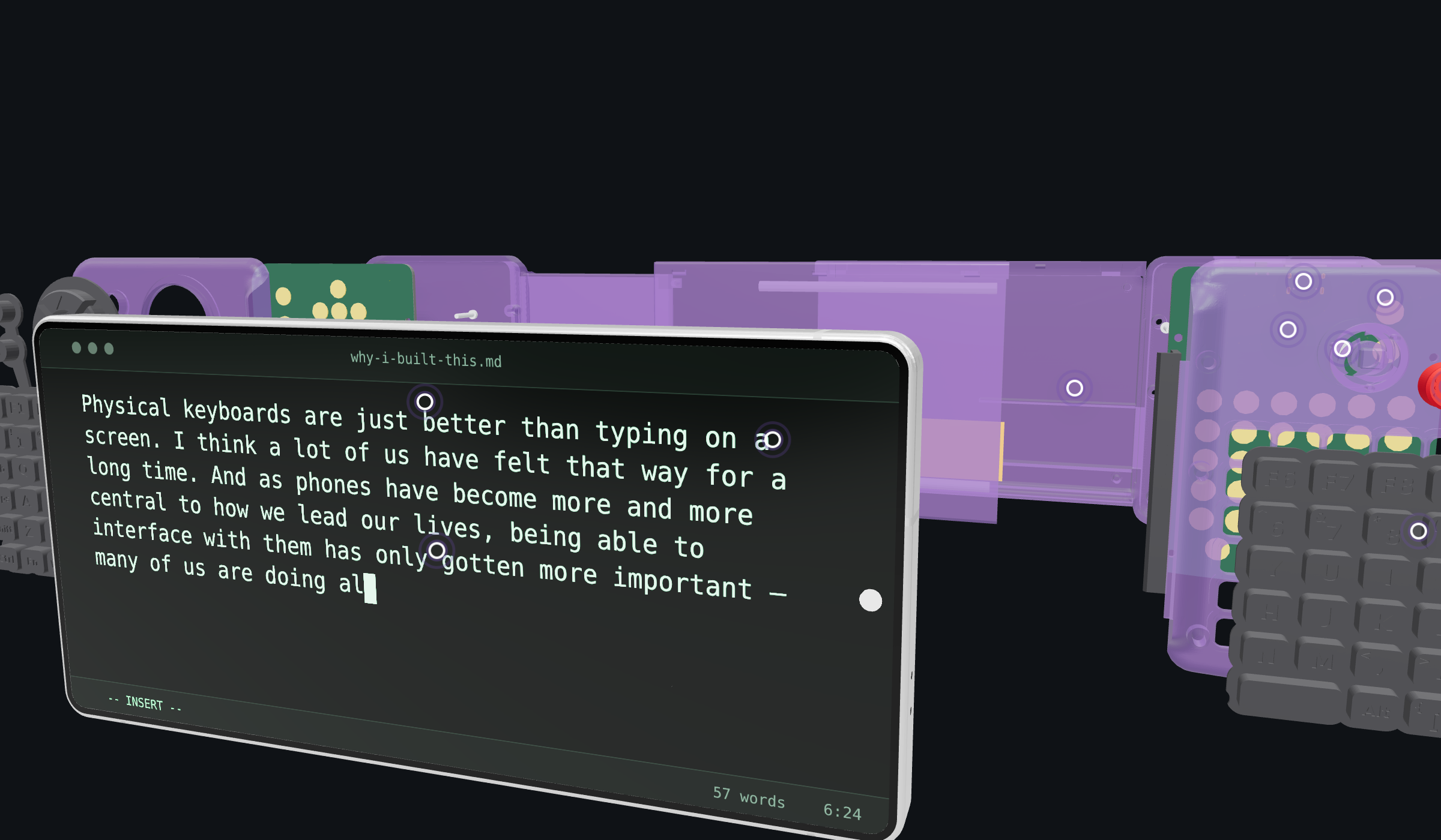
Full step-by-step in docs/assembly.md.
1. Order the boards. Regenerate the fab package (python3 hardware/scripts/gen_fab.py), then
upload fab/right/ and fab/left/ as two separate JLCPCB PCBA orders. Options: 4-layer, 1.6 mm
FR-4, ENIG, assembly side = bottom. The right board needs Standard assembly (the E73 is Extended);
the left can go Economic. Check the DFM preview for LED polarity and SOT-23/USB-C/E73 rotation before
paying. E73 stock is volatile — reserve C356849 before anything else.
2. Print and press. Shells in PETG, keymats in TPU 95A. Fatigue-test a 3×3 keymat coupon past 10 k cycles before committing a full mat. Press the 78 domes onto their pads under polyimide retention tape — the keymat alone will not stop a dome walking off its ring.
3. Assemble. FFC jumper first, before the lids go on: 20-way, type-A (contacts on the same side at both ends), contacts facing the board at both ends. Foam-tape the cell to the left grip floor before its board goes in, and meter the pigtail against the "+"/"−" silk at J4 on the left board — vendors wire PH pigtails both ways. Thread the ribbon through its walled tray lane before lapping the shrouds, press the TPU grippers onto the cradles, then the lids over them; 5× M2×12 per grip, driven from the back into the lid's inserts.
4. Flash. The E73 ships blank. One-time SWD flash of the Adafruit nRF52 bootloader (nice_nano
build) via TP1–5, possibly after nrfjprog --recover. This needs a debug probe and is the most
likely place to get stuck. After that it's drag-and-drop UF2 forever. Pair to the device
advertising as thumbdeck.
The clamp takes any 130–170 mm long edge out of the box. The interactive
viewer will seat a Galaxy S25 Ultra, an iPhone 17, an iPhone
Air or an iPhone 17 Pro Max in it and re-span the jaw to each — the Phone panel in the control bar.
The well itself is dimensioned for an S25 Ultra in a ~1.2 mm case; phone_w, phone_h, phone_t
and case_t in deck.py re-generate the shells for something else, and the PCBs are unaffected. A
substantially larger phone pushes the grips further apart than is comfortable to thumb-type across,
and moves the bridge connectors, so re-check the ribbon length.
| Path | What's in it |
|---|---|
hardware/scripts/ | The source of truth. deck.py is the parametric model; the rest generate boards, fab output, firmware and 2D renders from it |
hardware/kicad/ | The generated KiCad 9 boards. Nothing here is hand-drawn |
hardware/cad/ | CadQuery shells and keymats, watertight STLs, and the nested GLB assembly |
hardware/footprints/ | Custom footprints, including the snap-dome contact pad. Some are vendored — see NOTICE |
firmware/zmk-config/ | ZMK v0.3.0 config with a real board definition at config/boards/arm/thumbdeck/ |
docs/ | The engineering documents, indexed below |
renders/ · sketches/ · references/ | Generated images; the original concept drawings; Rii i8+ reference photos |
| I want to know… | Read |
|---|---|
| Why is it built this way, with rejected alternatives | docs/design-decisions.md |
| How to assemble one, in order | docs/assembly.md |
| What to buy, from whom, for how much | docs/fabrication-sourcing.md · docs/bill-of-materials.md |
| How the matrix works | docs/matrix-and-diodes.md |
| Battery, charging, USB, ESD, the FFC bridge | docs/connectivity-and-power.md |
| How Python turns into a routed PCB / printable shells | docs/routing-status.md · docs/cad-process.md |
| What an EE would tear apart | docs/design-review.md · docs/evaluation.md |
cd hardware/scripts
python3 gen_board.py                  # placement + netlist + USB copper + GND escape vias
./route.sh right && ./route.sh left   # Freerouting -> GND stitch + zone fill -> DRC gate
python3 gen_fab.py                    # gerbers/BOM/CPL per side (refuses unless DRC-clean)
python3 verify_alignment.py           # 2D stack audit: pads vs model, gutters, boss clearances
python3 sim_matrix.py                 # ghosting/NKRO proof
python3 gen_firmware.py               # ZMK transform/keymap/gpio
python3 layout_gen.py --iter 23       # layout diagram
python3 render_fab.py                 # fab view
# --- 3D (CadQuery) ---
cd ../.. && hardware/cad/.venv/bin/python hardware/cad/deck3d.py --all --check --render
hardware/cad/.venv/bin/python hardware/cad/export_full_asm.py   # full-assembly GLB
Needs Python 3 + matplotlib; the board pipeline needs KiCad 9 (pcbnew + kicad-cli) and a
Freerouting jar; the 3D generator uses a venv at hardware/cad/.venv/ built from
hardware/cad/requirements.txt.
Routing intermediates, DRC JSONs and fab/ are build artifacts and are not committed. Generated
files are outputs, not sources — don't hand-edit hardware/kicad/generated/,
hardware/cad/models/ or renders/; change the model and re-run.
Real decisions still on the table: a flat ortho grid vs a canted/fanned key arc; shoulder buttons for the index fingers; an I²C trackpad on the TP6–8 breakout (dropped from v1 over driver burden). A trackpad and shoulder buttons are both rev-B changes.
See CONTRIBUTING.md and CODE_OF_CONDUCT.md. The most valuable contribution right now is not code — it's a first-article build reported with photos, especially if it doesn't work. After that: ergonomic critique, a KiCad/RF review of the autorouted boards, and a ZMK review of the board definition.
There is no kit, no store and no waiting list. It's Apache 2.0, so build it, modify it or sell it yourself.
Apache License 2.0 — see LICENSE. Copyright © 2026 Eric Neuman.
Some files carry their own terms and are not relicensed: the two marbastlib-derived footprints
(CERN-OHL-P-2.0), stock KiCad footprints (CC-BY-SA-4.0 with the library exception), the phone GLB
and the references/ photos (provenance not established — establish it or remove them before
redistributing). Details in NOTICE and
docs/reference-notes.md.
"Rii" is a trademark of its owner; this project is not affiliated with or endorsed by Rii. No i8+ artwork, geometry, footprint or firmware was copied into this design.
| Qty | Value | Footprint | References |
|---|---|---|---|
| 36 | 1N4148WS | D_SOD-323 | D1, D2, D10, D11, D12, D13, D14, D15, D16, D17, D18, D19, D20, D21, D22, D23 +20 |
| 36 | SNAP7 | snaptron_7mm_contact | SW1, SW2, SW10, SW11, SW12, SW13, SW14, SW15, SW16, SW17, SW18, SW19, SW20, SW21, SW22, SW23 +20 |
| 11 | 4k7 | R_0402_1005Metric | R1, R2, R3, R4, R5, R6, R7, R8, R9, R26, R27 |
| 3 | 100nF | C_0402_1005Metric | C2, C6, C8 |
| 3 | 4u7/0805 | C_0805_2012Metric | C3, C4, C5 |
| 3 | 5k1 | R_0402_1005Metric | R20, R21, R24 |
| 2 | 1M | R_0402_1005Metric | R22, R23 |
| 2 | 1uF | C_0402_1005Metric | C1, C7 |
| 1 | 1k | R_0402_1005Metric | R25 |
| 1 | 3V3 | TestPoint_Pad_1.5x1.5mm | TP4 |
| 1 | E73-2G4M08S1C | nRF52840_E73-2G4M08S1C | U1 |
| 1 | FFC20 | ffc_afa07_s20fcc | J2 |
| 1 | GND | TestPoint_Pad_1.5x1.5mm | TP5 |
| 1 | LED_RED | LED_0603_1608Metric | D80 |
| 1 | MCP73831 | SOT-23-5 | U2 |
| 1 | MSK12C02 | msk12c02_slide | SW90 |
| 1 | RESET | TestPoint_Pad_1.5x1.5mm | TP3 |
| 1 | SCL | TestPoint_Pad_1.5x1.5mm | TP7 |
| 1 | SDA | TestPoint_Pad_1.5x1.5mm | TP6 |
| 1 | SWDCLK | TestPoint_Pad_1.5x1.5mm | TP2 |
| 1 | SWDIO | TestPoint_Pad_1.5x1.5mm | TP1 |
| 1 | TMAG5273 | SOT-23-6 | U4 |
| 1 | TP_INT | TestPoint_Pad_1.5x1.5mm | TP8 |
| 1 | TS-1187A | SW_Push_1P1T_XKB_TS-1187A | SW91 |
| 1 | USB-C | USB_C_Receptacle_HRO_TYPE-C-31-M-12 | J1 |
| 1 | USBLC6-2SC6 | SOT-23-6 | U3 |
neuman/gripster
thumbdeck — wireless split thumb keyboard (nRF52840 + ZMK, BLE split, i8+-inspired). Layout converged & graded PASS.


kartben/hw-testing-rack
3D-printed, tilted test shelf for 16 dev boards: sliding drawers, per-bay ESP32-S3 running Zephyr (USB/IP, power switching, metering), KiCad PCBs, OpenSCAD parts, BOM and an interactive 3D viewer

wallago/chocofi-PCB
KiCad PCB design for the chocofi, a 34-key wireless split keyboard

Mposiblee/Zireael
The keyboard is based on Dao Chok BLE. The locations of components on the board have been changed, space for the battery has been added, and the thumb cluster has also been changed.


FugLong/OpenChord
An open-source music device for portable, expressive, and extensible audio creation.

It measures 71.9 × 94 mm and has 4 copper layers, 1.6 mm thick.
114 parts, built around the E73-2G4M08S1C, MCP73831, USBLC6-2SC6 and 1N4148WS. The full list of its parts is on this page, with links to each part's symbol and footprint where PCBKit's library has them.
From the neuman/gripster repository on GitHub, at the commit this page was made from: the board is hardware/kicad/generated/thumbdeck_right.kicad_pcb. PCBKit opens the board in the browser, with nothing to install.
Its repository publishes it under the Apache-2.0 licence: you may reuse it on that licence's terms (keep the author's notice, and for a copyleft licence share your changes alike).