

6 layers100 × 100 mm
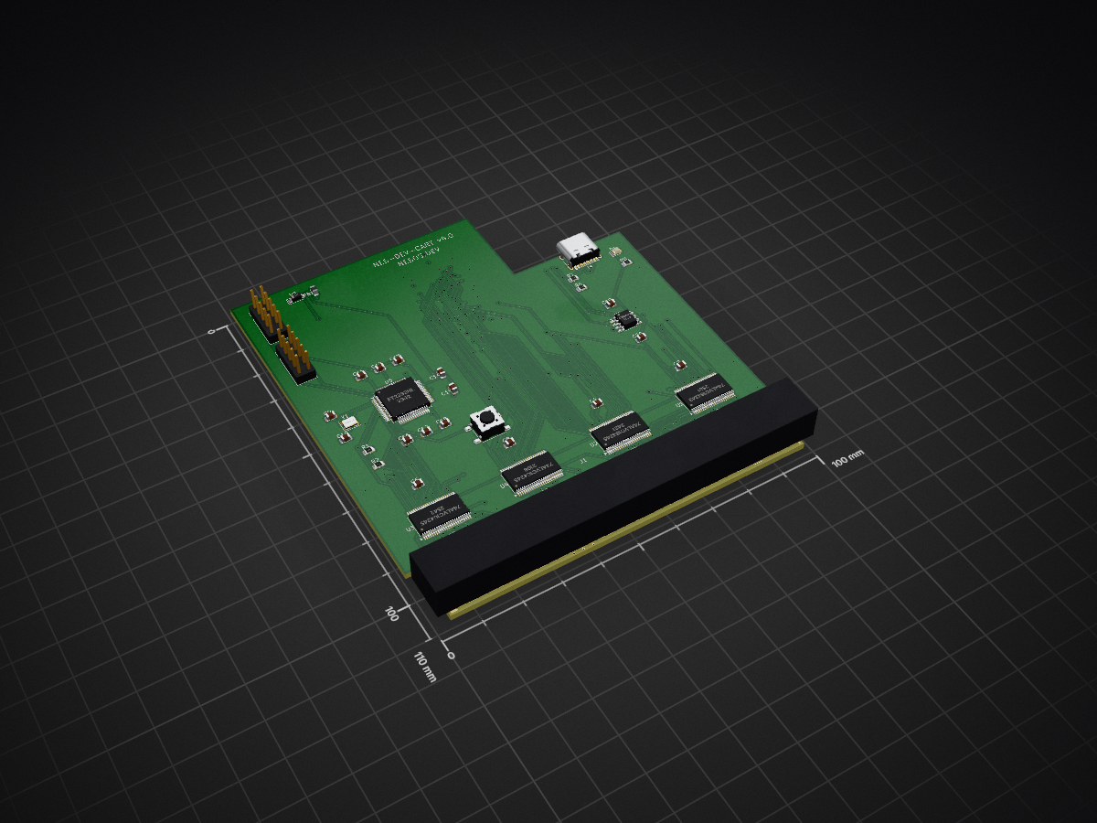
 nesos-dev/nes-dev-cart8
NES-DEV-CART: Open-source FPGA development cartridge for the Nintendo Entertainment System
Nes dev cart is an open-source printed circuit board by nesos-dev, from the nesos-dev/nes-dev-cart repository on GitHub, published under the GPL-3.0 licence. It is a 4-layer board of 100 × 110 mm with 42 parts on 157 nets, routed with 1,853 tracks and 360 vias.
It is built around the 74ALVC164245DL and FT2232HL. Its parts include 20 capacitors, 6 ICs, 6 connectors, 5 resistors and 2 diodes. It belongs with the retro computing and games and fPGA and programmable logic boards of this library.
Open-source FPGA development cartridge for the Nintendo Entertainment System. v4.1 — now with 8MB onboard PSRAM.
Plugs into a real NES. Programs over USB-C. Debug via UART. Full NES bus access. 39 SMT components, professionally assembled.
NES-DEV-CART is a cartridge-shaped PCB that replaces the ROM chip with a modern FPGA. It gives your FPGA bidirectional access to every signal on the NES 72-pin cartridge connector — CPU bus, PPU bus, CIC, expansion port — all level-shifted between 5V and 3.3V.
An onboard FT2232HL provides USB-C JTAG programming and UART debug console. No external programmer needed.
| FPGA | Sipeed Tang Primer 25K (Gowin GW5A-25, 25K LUTs) |
| ROM Storage | 8MB SPI PSRAM |
| USB | FT2232HL — Ch.A: JTAG, Ch.B: UART debug |
| Level Shifting | 4x 74ALVC164245DGG (bidirectional 5V-3.3V) |
| NES Signals | CPU A0-A14, D0-D7, PPU A0-A13, D0-D7, CIC, IRQ, EXP |
| PCB | 4-layer, 1.6mm, ENIG, gold fingers, L-shaped |
| Connector | 72-pin NES edge connector (30-degree bevel) |
| FPGA Connection | 2x DF40C-60DS 0.4mm B2B connectors |
hardware/
├── nes-dev-cart.kicad_pcb      KiCad PCB layout
├── nes-dev-cart.kicad_sch      KiCad schematic
├── nes-dev-cart.kicad_pro      KiCad project
├── footprints/                 Custom footprint libraries
├── shell/                     Cart shell STL files (front/back)
└── production/
    ├── nes-dev-cart-gerbers.zip    Fabrication-ready gerbers
    ├── nes-dev-cart-bom.csv        BOM with LCSC part numbers
    ├── nes-dev-cart-cpl-jlcpcb.csv Component placement list
    ├── README-assembly.md          Assembly instructions
    ├── nes-dev-cart-render-*.png   Board renders (top/bottom)
    └── gerbers/                    Individual gerber files

website/                        Product website (nesos.dev)
├── index.html
├── style.css
└── success.htmlUpload hardware/production/nes-dev-cart-gerbers.zip to JLCPCB:
Upload nes-dev-cart-bom.csv and nes-dev-cart-cpl-jlcpcb.csv for SMT assembly. See production/README-assembly.md for details.
Hardware: GPL-3.0
NES-DEV-CART is an independent project not affiliated with or endorsed by Nintendo.
| Qty | Value | Footprint | References |
|---|---|---|---|
| 15 | 100nF | Capacitor_SMD:C_0805_2012Metric | C1, C2, C3, C4, C5, C6, C7, C8, C11, C12, C13, C14, C16, C18, C19 |
| 4 | 74ALVC164245 | Package_SO:TSSOP-48_6.1x12.5mm_P0.5mm | U1, U2, U3, U4 |
| 2 | 27pF | Capacitor_SMD:C_0805_2012Metric | C9, C10 |
| 2 | 4.7uF | Capacitor_SMD:C_0805_2012Metric | C15, C17 |
| 2 | 5.1k | Resistor_SMD:R_0805_2012Metric | R3, R4 |
| 2 | DF40C-60DS | DF40C-60DS | J2, J3 |
| 1 | 10k | Resistor_SMD:R_0805_2012Metric | R2 |
| 1 | 10uF | Capacitor_SMD:C_0805_2012Metric | C20 |
| 1 | 12MHz | Crystal:Crystal_SMD_3225-4Pin_3.2x2.5mm | Y1 |
| 1 | 1N5817 | Diode_SMD:D_SOD-123 | D2 |
| 1 | 2.2k | Resistor_SMD:R_0805_2012Metric | R1 |
| 1 | 330 | Resistor_SMD:R_0805_2012Metric | R5 |
| 1 | APS6404L | Package_SO:SOIC-8_3.9x4.9mm_P1.27mm | U6 |
| 1 | EXPANSION | Connector_PinHeader_2.54mm:PinHeader_2x05_P2.54mm_Vertical | J6 |
| 1 | FT2232HL | Package_QFP:LQFP-64_10x10mm_P0.5mm | U5 |
| 1 | Ferrite | Inductor_SMD:L_0805_2012Metric | FB1 |
| 1 | JTAG | Connector_PinHeader_2.54mm:PinHeader_2x05_P2.54mm_Vertical | J5 |
| 1 | LED | LED_SMD:LED_0805_2012Metric | D1 |
| 1 | NES_72Pin | NES_72Pin_CardEdge | J1 |
| 1 | RESET | Button_Switch_SMD:SW_SPST_PTS645Sx43SMTR92 | SW1 |
| 1 | USB_C | Connector_USB:USB_C_Receptacle_HRO_TYPE-C-31-M-12 | J4 |
It measures 100 × 110 mm and has 4 copper layers, 1.6 mm thick.
42 parts, built around the 74ALVC164245DL and FT2232HL. The full list of its parts is on this page, with links to each part's symbol and footprint where PCBKit's library has them.
From the nesos-dev/nes-dev-cart repository on GitHub, at the commit this page was made from: the board is hardware/nes-dev-cart.kicad_pcb and its schematic hardware/nes-dev-cart.kicad_sch. PCBKit opens the board in the browser, with nothing to install.
Its repository publishes it under the GPL-3.0 licence: you may reuse it on that licence's terms (keep the author's notice, and for a copyleft licence share your changes alike).


Xeraster/32bit_486_motherboard
A completely DIY 486 motherboard. Even the chipset is a DIY fpga thing. This version has a 32 bit front side bus and a 16 bit ISA bis


teknoman117/M68K-BUS-VOLTAGE-CONVERTER
A breakout board for the MC68010 which converts the 5V bus to a 3.3V bus you can connect to an FPGA

ianhan/graphics-gremlin-gizmo
This is a modified version of the Graphics Gremlin ISA CGA/MDA graphics card to include a HDMI port.


viuhimciuc/coolgirl-nes-multicart
Ultimate multigame cartridge for Nintendo Entertainment System (NES)