2 layers27.9 × 16.5 mm
 Nam2302/Hackpad
Top Case PCB Case Bottom Case Made in Tinkercad
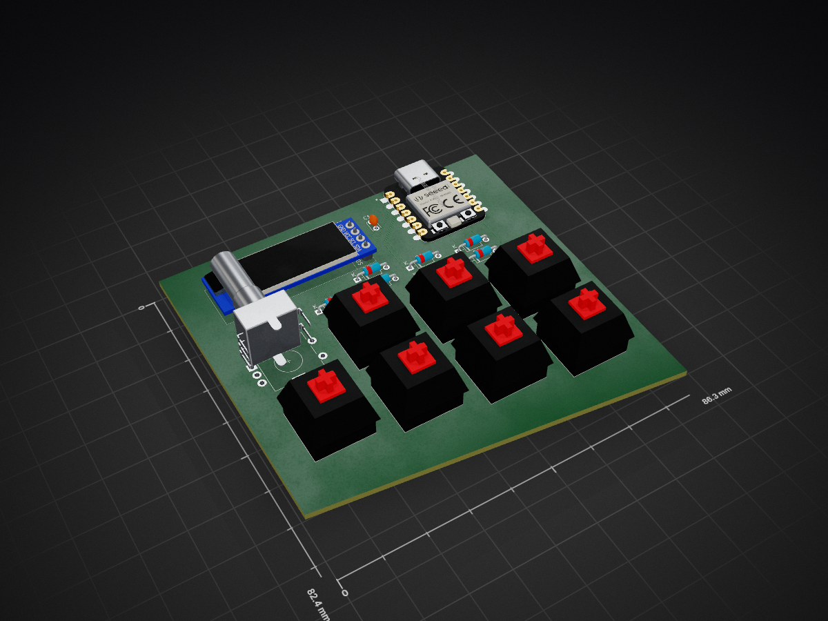
Hackpad is an open-source printed circuit board by Nam2302, from the Nam2302/Hackpad repository on GitHub. It is a 2-layer board of 86.3 × 82.4 mm with 18 parts on 21 nets, routed with 97 tracks and 0 vias.
Its parts include 8 switches, 7 diodes, 1 capacitor, 1 IC and 1 connector.
The Hackpad has 8-inputs (7 switches + rotary encoder) with an OLED display. It uses QMK firmware, and the layout includes simple and frequently used shortcuts.
 |  |
| Schematic | PCB |
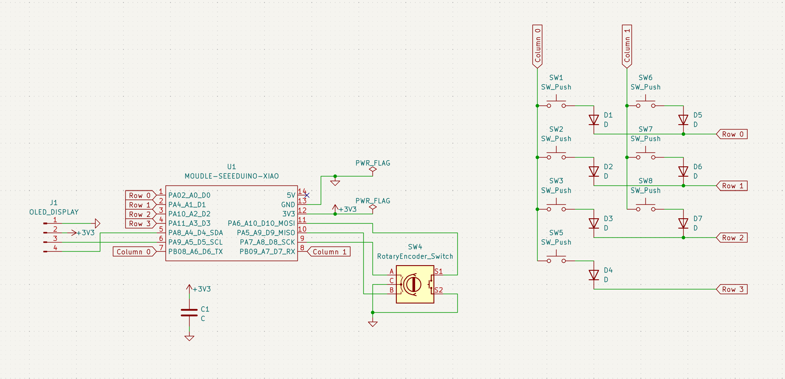 | 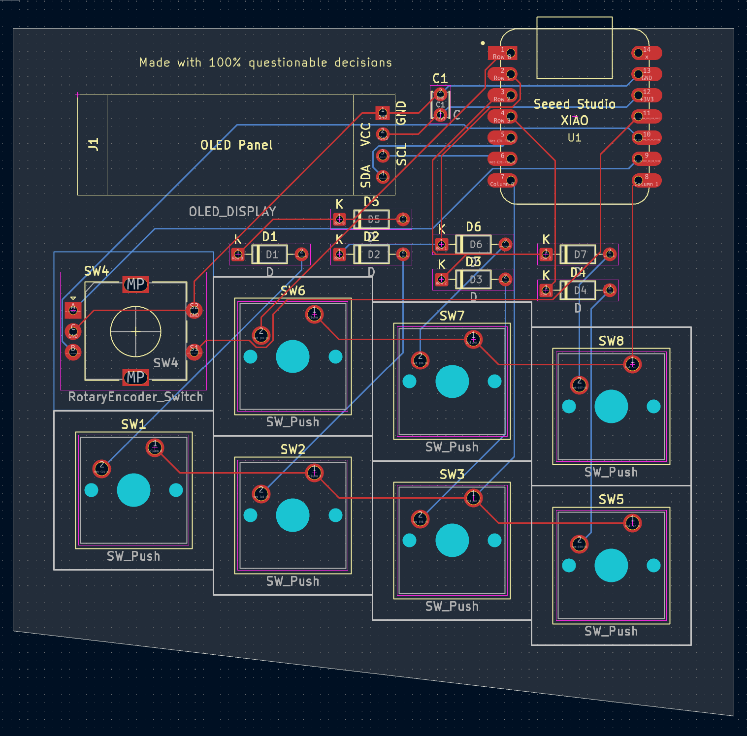 |
Made in KiCad
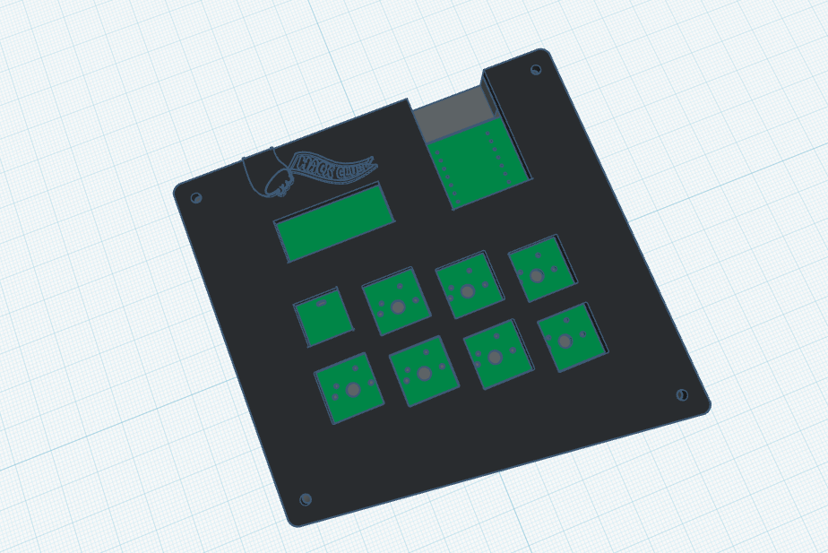
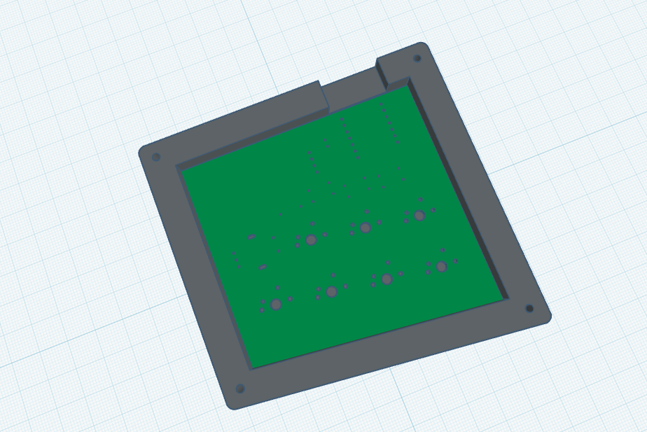
The case has two pieces, which includes the top switch plate and a bottom container. Inside it is a cavity where the PCB sits. The design also has a distinct diagonal edge on the bottom.
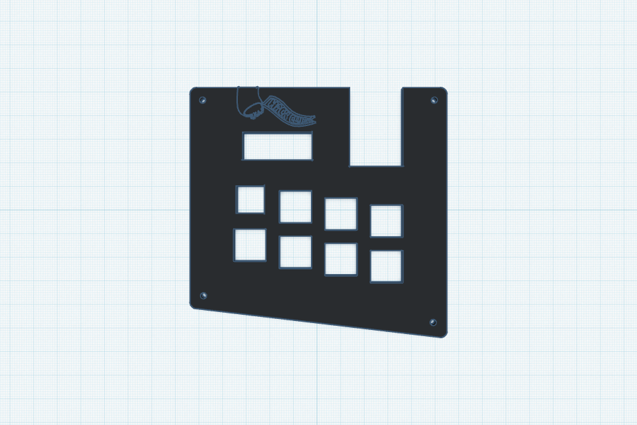 | Top Case |
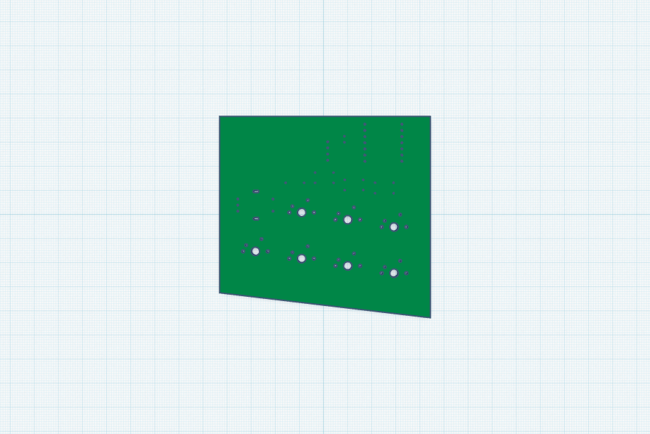 | PCB Case |
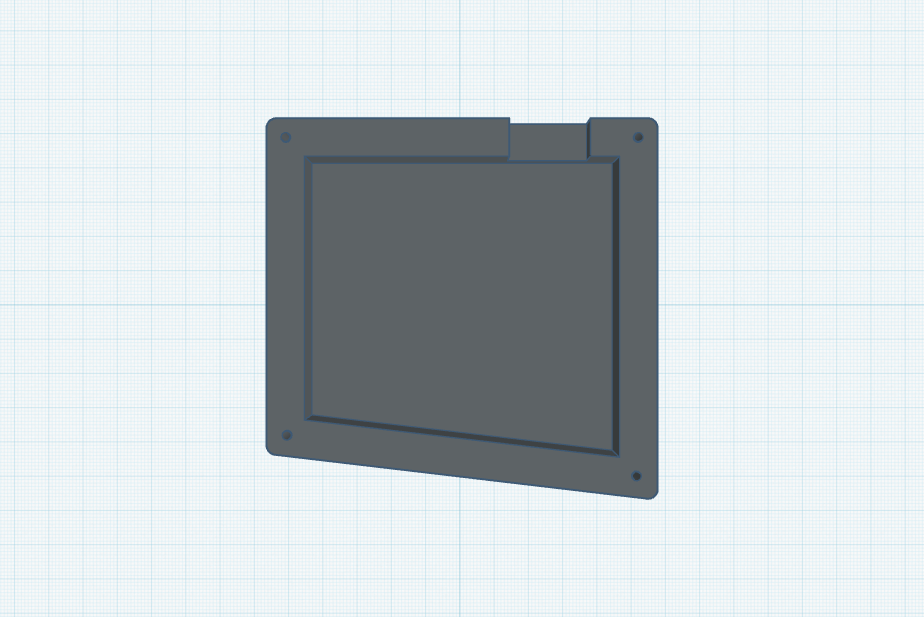 | Bottom Case |
Made in Tinkercad
This Hackpad runs QMK firmware. There's a single layer with 7 keys mapped to the following shortcuts: new tab, new window, undo, redo, refresh, paste, and copy, with the encoder controlling volume. The OLED currently displays a simple status message.
This was the first PCB and CAD project I've ever finished, and had many challenges. I redesigned the PCB layout three separate times trying to get it under the 100x100mm size limit. The case design also had hurdles as I mostly started out eyeballing every measurement by dragging shapes around in Tinkercad, which never quite lined up right. I redid the whole thing once I actually found the align tool and coordinate input fields. Finally, setting up Ubuntu to get the firmware going was a whole separate issue, but overall I am proud of my journey and final product.
Here is everything you need to create this Hackpad:
| Component | Amount |
|---|---|
| Seeed XIAO RP2040 | 1x |
| MX-Style switches (Cherry MX 1.00u) | 7x |
| 1N4148 Diodes | 7x |
| EC11 Rotary encoder | 1x |
| 0.91 inch OLED display | 1x |
| DSA keycaps | 7x |
| 100nF Ceramic capacitor | 1x |
| M3x16mm screw | 4x |
| Case (2 printed parts) | 1x |
| PCB | 1x |
| Qty | Value | Footprint | References |
|---|---|---|---|
| 7 | D | Diode_THT:D_DO-35_SOD27_P7.62mm_Horizontal | D1, D2, D3, D4, D5, D6, D7 |
| 7 | SW_Push | Button_Switch_Keyboard:SW_Cherry_MX_1.00u_PCB | SW1, SW2, SW3, SW5, SW6, SW7, SW8 |
| 1 | C | Capacitor_THT:C_Disc_D3.0mm_W2.0mm_P2.50mm | C1 |
| 1 | MOUDLE-SEEEDUINO-XIAO | footprints:XIAO-Generic-Hybrid-14P-2.54-21X17.8MM | U1 |
| 1 | OLED_DISPLAY | oled:SSD1306-0.91-OLED-4pin-128x32 | J1 |
| 1 | RotaryEncoder_Switch | Rotary_Encoder:RotaryEncoder_Alps_EC11E-Switch_Vertical_H20mm | SW4 |
It measures 86.3 × 82.4 mm and has 2 copper layers, 1.6 mm thick.
18 parts. The full list of its parts is on this page, with links to each part's symbol and footprint where PCBKit's library has them.
From the Nam2302/Hackpad repository on GitHub, at the commit this page was made from: the board is PCB/HackPad.kicad_pcb and its schematic PCB/HackPad.kicad_sch. PCBKit opens the board in the browser, with nothing to install.
Its repository states no licence, so its author keeps all rights: ask Nam2302 before reusing the design.

VoronDesign/Voron-Hardware
Cool Hardware designed by the Voron Design group


hackclub/OnBoard
💡 Join 1,000 teenagers and make your first PCB with a $100 grant!

VoronDesign/Voron-Tap
Tap is a nozzle-based z-probe for the V2 and Trident printer designs. The entire toolhead moves to trigger an optical switch. Tap offers many advantages:

Luos-io/luos_engine
Open-source and real-time orchestrator for cyber-physical-systems, to easily design, test and deploy embedded applications and digital twins.


Twotoz/C5VRX
Ultra-minimal, zero-CPU 5.8 GHz analog FPV video receiver using ESP32-C5 Wi-Fi 6 PHY MODEM_DIAG, BitScrambler WBFM demodulation & resistor DAC CVBS