4 layers32.5 × 105.2 mm
ZESP32
zmaker/arduino_cookbook
gli sketch del nuovo progetto Arduino Cookbook e dei video di YouTube
42 parts269

 mwrnd/PCIe_x8_Breakout6
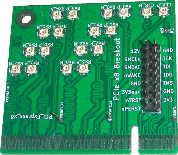
PCIe x8 Signal Breakout to U.FL/UMCC Connectors
PCIe x8 Breakout is an open-source printed circuit board by mwrnd, from the mwrnd/PCIe_x8_Breakout repository on GitHub, published under the BSD-2-Clause licence. It is a 4-layer board of 47.7 × 51.3 mm with 42 parts on 56 nets, routed with 1,307 tracks and 160 vias.
Its parts include 36 connectors and 1 resistor. It belongs with the computers and single-board computers and interfaces and adapters boards of this library.
PCIe x8 Signal Breakout to U.FL/UMCC Connectors.
PCIEX1-SMA is a similar project that is PCIe x1 and uses SMA connectors.
The board requires up to 34 U.FL/UMCC Surface Mount Receptacles and a 16-Pin 2.54mm Header or Socket.
Related Projects: OpenCAPI_Breakout, OpenCAPI-to-PCIe, OpenCAPI-to-PCIe_x4_Host_and_Endpoint
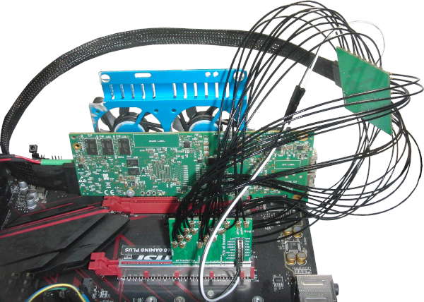
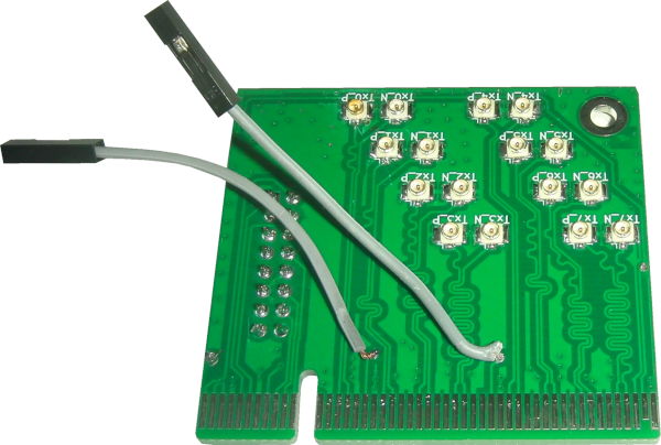
The board is currently being used along with an OpenCAPI_Breakout board to test OpenCAPI-to-PCIe on the Innova-2 SmartNIC. PCIe 3.0 x4 at 8.0GT/s is currently working. Standard 0.1" M-F Jumpers are used for the PCIe Reset Signal (nPERST) and its GND.
With cables shorter than 4"~=100mm the adapters work. Note the RX U.FL-to-U.FL cables are all the same length as each other and likewise all TX cables are the same length but RX and TX are different lengths as that is what I had access to. RX on the PCIe board connects to RX on the OpenCAPI board as it uses the OpenCAPI Host pinout.
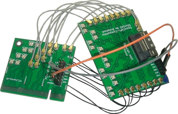
PCIe x4 In-system:
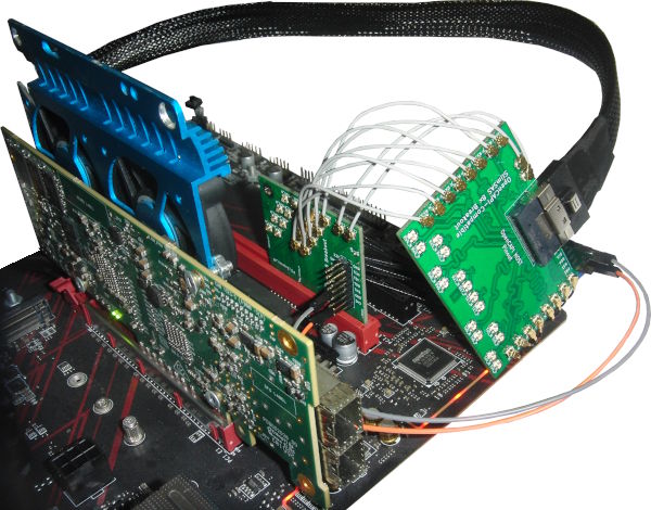
However, using 250mm IPEX cables the adapters fail for PCIe x8:
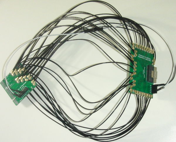
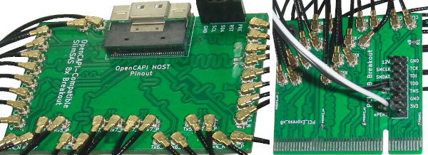
PCIe x8 In-system:
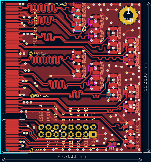
All signals are length-matched to within 1mm both inter-pair and intra-pair.
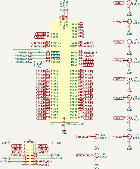
Resistor footprint R1 connects PRSNT1 to PRSNT2_x8. The R1 trace can be cut and PRSNT1 can be connected to a different PRSNT2 to reduce the PCIe lane width.
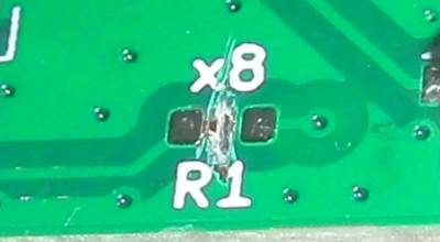
Wire jumpers can then be used to connect PRSNT1 to any of the PRSNT2.
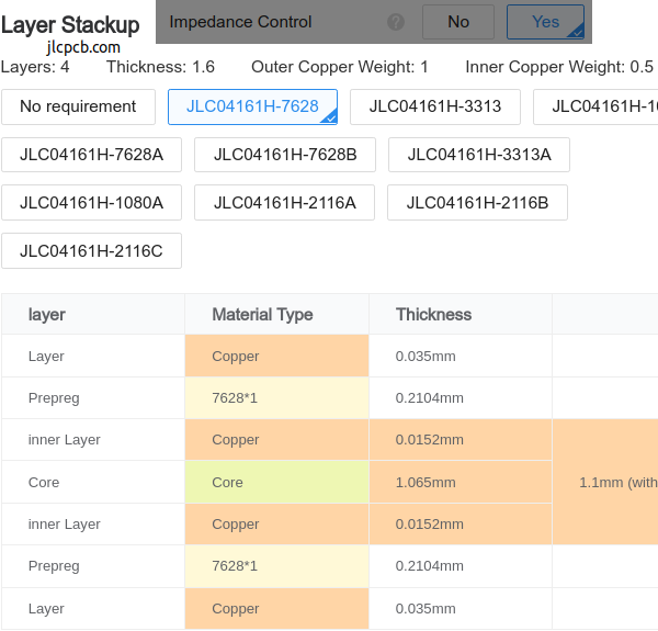
4-Layer PCB stackup taken from JLCPCB.
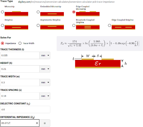
Differential Impedance parameters were calculated using the DigiKey Online Calculator.
| Qty | Value | Footprint | References |
|---|---|---|---|
| 1 | CLK_N | U.FL_w_Label:U.FL_Hirose_w_Label | J36 |
| 1 | CLK_P | U.FL_w_Label:U.FL_Hirose_w_Label | J35 |
| 1 | Conn_02x08_Odd_Even | Connector_PinSocket_2.54mm:PinSocket_2x08_P2.54mm_Vertical | J7 |
| 1 | DNP | Resistor_SMD:R_0603_1608Metric | R1 |
| 1 | GND | Connector_PinSocket_2.54mm:PinSocket_1x01_P2.54mm_Vertical | TP1 |
| 1 | PCI_Express_x8 | Connector_PCBEdge:BUS_PCIexpress_x8 | J1 |
| 1 | PRSNT1 | Connector_PinHeader_1.00mm:PinHeader_1x01_P1.00mm_Vertical | TP6 |
| 1 | PRSNT2_x1 | Connector_PinHeader_1.00mm:PinHeader_1x01_P1.00mm_Vertical | TP7 |
| 1 | PRSNT2_x4 | Connector_PinHeader_1.00mm:PinHeader_1x01_P1.00mm_Vertical | TP8 |
| 1 | PRSNT2_x8 | Connector_PinHeader_1.00mm:PinHeader_1x01_P1.00mm_Vertical | TP9 |
| 1 | Rx0_N | U.FL_w_Label:U.FL_Hirose_w_Label | J4 |
| 1 | Rx0_P | U.FL_w_Label:U.FL_Hirose_w_Label | J3 |
| 1 | Rx1_N | U.FL_w_Label:U.FL_Hirose_w_Label | J5 |
| 1 | Rx1_P | U.FL_w_Label:U.FL_Hirose_w_Label | J2 |
| 1 | Rx2_N | U.FL_w_Label:U.FL_Hirose_w_Label | J8 |
| 1 | Rx2_P | U.FL_w_Label:U.FL_Hirose_w_Label | J6 |
| 1 | Rx3_N | U.FL_w_Label:U.FL_Hirose_w_Label | J10 |
| 1 | Rx3_P | U.FL_w_Label:U.FL_Hirose_w_Label | J9 |
| 1 | Rx4_N | U.FL_w_Label:U.FL_Hirose_w_Label | J12 |
| 1 | Rx4_P | U.FL_w_Label:U.FL_Hirose_w_Label | J11 |
| 1 | Rx5_N | U.FL_w_Label:U.FL_Hirose_w_Label | J14 |
| 1 | Rx5_P | U.FL_w_Label:U.FL_Hirose_w_Label | J13 |
| 1 | Rx6_N | U.FL_w_Label:U.FL_Hirose_w_Label | J16 |
| 1 | Rx6_P | U.FL_w_Label:U.FL_Hirose_w_Label | J15 |
| 1 | Rx7_N | U.FL_w_Label:U.FL_Hirose_w_Label | J18 |
| 1 | Rx7_P | U.FL_w_Label:U.FL_Hirose_w_Label | J17 |
| 1 | Tx0_N | U.FL_w_Label:U.FL_Hirose_w_Label | J20 |
| 1 | Tx0_P | U.FL_w_Label:U.FL_Hirose_w_Label | J19 |
| 1 | Tx1_N | U.FL_w_Label:U.FL_Hirose_w_Label | J22 |
| 1 | Tx1_P | U.FL_w_Label:U.FL_Hirose_w_Label | J21 |
| 1 | Tx2_N | U.FL_w_Label:U.FL_Hirose_w_Label | J24 |
| 1 | Tx2_P | U.FL_w_Label:U.FL_Hirose_w_Label | J23 |
| 1 | Tx3_N | U.FL_w_Label:U.FL_Hirose_w_Label | J26 |
| 1 | Tx3_P | U.FL_w_Label:U.FL_Hirose_w_Label | J25 |
| 1 | Tx4_N | U.FL_w_Label:U.FL_Hirose_w_Label | J28 |
| 1 | Tx4_P | U.FL_w_Label:U.FL_Hirose_w_Label | J27 |
| 1 | Tx5_N | U.FL_w_Label:U.FL_Hirose_w_Label | J30 |
| 1 | Tx5_P | U.FL_w_Label:U.FL_Hirose_w_Label | J29 |
| 1 | Tx6_N | U.FL_w_Label:U.FL_Hirose_w_Label | J32 |
| 1 | Tx6_P | U.FL_w_Label:U.FL_Hirose_w_Label | J31 |
| 1 | Tx7_N | U.FL_w_Label:U.FL_Hirose_w_Label | J34 |
| 1 | Tx7_P | U.FL_w_Label:U.FL_Hirose_w_Label | J33 |
zmaker/arduino_cookbook
gli sketch del nuovo progetto Arduino Cookbook e dei video di YouTube

rjwalters/kicad-tools
Standalone Python tools for parsing and manipulating KiCad schematic and PCB files

Eidon-AI/eidon-glove
A robust 16-DOF hand/finger tracking wearable standard Bluetooth Human Interface Device (BLE HID) designed for humanoid teleoperation and collecting embodied AI training datasets.

calithameridi/corevus
High-flexibility, low-cost mechatronics controller for 3D printers

Squantor/templates_kicad
Kicad templates that I use regularly

garrettsworkshop/MacIIROMSIMM
ROM SIMM for Apple Macintosh II-series and Macintosh SE/30 machines

oresat/oresat-live-handheld-ground-station
MCAD, ECAD, software, firmware, build instructions, and everything else you should need for the OreSat Live Handheld Ground Station project.

It measures 47.7 × 51.3 mm and has 4 copper layers, 1.61 mm thick.
42 parts. The full list of its parts is on this page, with links to each part's symbol and footprint where PCBKit's library has them.
From the mwrnd/PCIe_x8_Breakout repository on GitHub, at the commit this page was made from: the board is PCIe_x8_Breakout.kicad_pcb and its schematic PCIe_x8_Breakout.kicad_sch. PCBKit opens the board in the browser, with nothing to install.
Its repository publishes it under the BSD-2-Clause licence: you may reuse it on that licence's terms (keep the author's notice, and for a copyleft licence share your changes alike).