2 layers105 × 105 mm
Neopixel
hackclub/OnBoard
💡 Join 1,000 teenagers and make your first PCB with a $100 grant!
71 parts915

 muritai97/blaster
4+5*3+2+1 split keyboard (WIP)
Blaster is an open-source printed circuit board by muritai97, from the muritai97/blaster repository on GitHub, published under the MIT licence. It is a 2-layer board of 173.4 × 115.8 mm with 71 parts on 44 nets, routed with 699 tracks and 59 vias.
Its parts include 23 diodes and 23 switches. It belongs with the keyboards and input boards of this library.
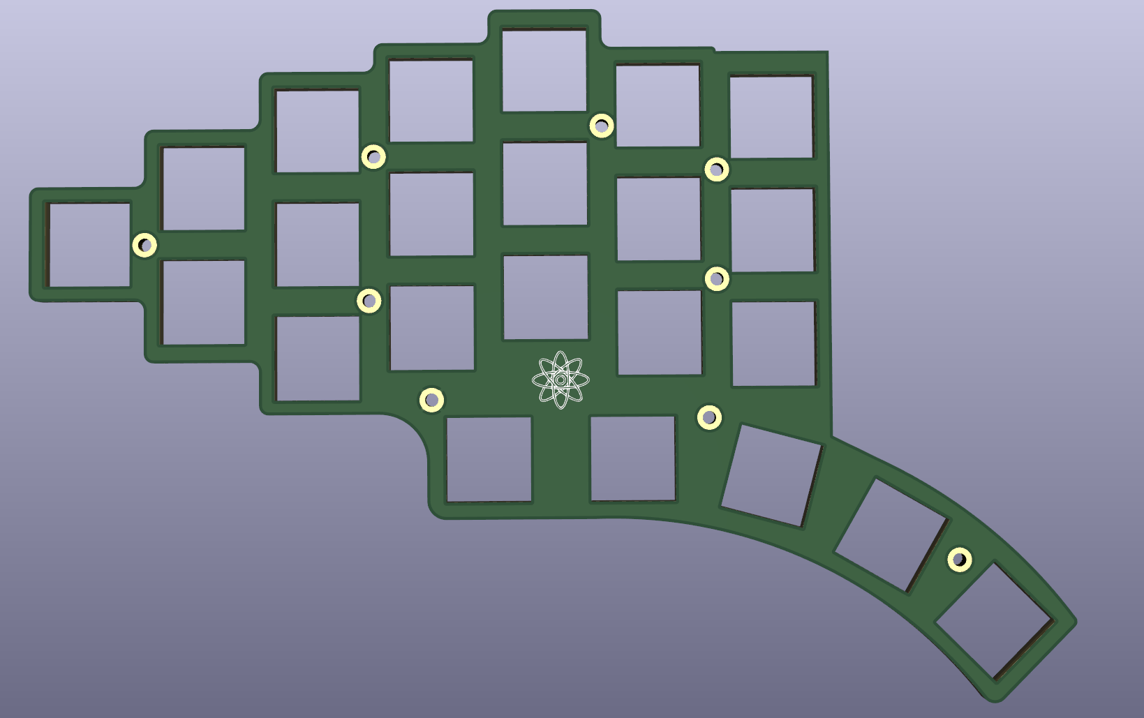
4+5*3+2+1 split keyboard (WIP)
layout mockup - optional encoder in place of left-most thumbcluster
| Qty | Value | Footprint | References |
|---|---|---|---|
| 23 | MX | S24, S25, S26, S27, S28, S29, S30, S31, S32, S33, S34, S35, S36, S37, S38, S39 +7 | |
| 23 | ComboDiode | D1, D2, D10, D11, D12, D13, D14, D15, D16, D17, D18, D19, D20, D21, D22, D23 +7 | |
| 12 | , , , , , , , , , , , | ||
| 8 | Jumper:SolderJumper-2_P1.3mm_Open_Pad1.0x1.5mm | , , , , , , , | |
| 1 | MCU_RaspberryPi_and_Boards:RPi_Pico_SMD_TH | this side up | |
| 1 | Rotary_Encoder:RotaryEncoder_Alps_EC11E-Switch_Vertical_H20mm | ||
| 1 | 128x64OLED | SSD1306:128x64OLED | SSD1306 |
| 1 | TRRS-PJ-320A-dual | TRRS-PJ-320A-dual | TRRS1 |
| 1 | this side down | ProMicro | MCU1 |
It measures 173.4 × 115.8 mm and has 2 copper layers, 1.6 mm thick.
71 parts. The full list of its parts is on this page, with links to each part's symbol and footprint where PCBKit's library has them.
From the muritai97/blaster repository on GitHub, at the commit this page was made from: the board is blaster/blaster.kicad_pcb and its schematic blaster/blaster.kicad_sch. PCBKit opens the board in the browser, with nothing to install.
Its repository publishes it under the MIT licence: you may reuse it on that licence's terms (keep the author's notice, and for a copyleft licence share your changes alike).
hackclub/OnBoard
💡 Join 1,000 teenagers and make your first PCB with a $100 grant!


hydrabus/hydrabus
HydraBus open source multi-tool for anyone interested in learning/developping/debugging/hacking/Penetration Testing for basic or advanced embedded hardware

beekeeb/Allium58
The Allium58 is created based on the Lily58 Pro, designed to enhance wireless capabilities and provide compatibility with GLP (Gateron Low Profile) hotswap sockets.


siderakb/ergo-snm-keyboard
ErgoSNM is a split ergonomic keyboard integrated with trackball, wireless is in beta

cnlohr/cnhardware
My dumping grounds for all my kicad projects and random hardware bringup.