Skip to the content
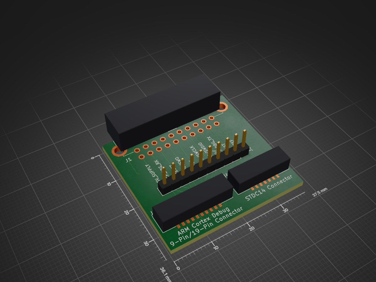
2 layers37.5 × 36.1 mmJ Link Ultra Cortex Adapter, the printed circuit board in 3D

Improved adapter PCB from SEGGER J-Link to Cortex Debug cable

Size
37.5 × 36.1 mm
Copper layers
2
Thickness
1.6 mm
Parts
7
Nets
24
Pads
71
Tracks, vias
145, 13
Pours
1
Routed
Yes
KiCad
KiCad 8.0 (file 20240108)
Created
27 Jul 2024
Updated
1 Nov 2024

Overview

J Link Ultra Cortex Adapter is an open-source printed circuit board by multiplemonomials, from the multiplemonomials/J-Link-Ultra-Cortex-Adapter repository on GitHub. It is a 2-layer board of 37.5 × 36.1 mm with 7 parts on 24 nets, routed with 145 tracks and 13 vias.

It is built around the SFH11-PBPC-D10-RA-BK. It belongs with the interfaces and adapters boards of this library.

Main components

1

README

README.md

J-Link Ultra Cortex Adapter

J-Links, as debug probes, are amazing. They can talk to just about any processor, ARM or otherwise, in common use in the last decade. The huge breadth of software and hardware compatibility available from one debug probe plus a set of adapters is incredible, and SEGGER deserves credit for getting this right.

Except... one thing. The adapters they sell for connecting a J-Link to a 9-pin or 19-pin Cortex-Debug connector are just... bad. They are bad, in fact, in several ways:

  • They are expensive. $40 for a tiny PCB with two connectors on it is too much.
  • They don't connect the VCP (Virtual COM Port) pins. Having a UART available to talk to the target device is a super useful feature of newer J-Links, but the design of these adapters just ignores it. In fact, they don't even break the pins out, so they it's impossible to access without sketchy bodge wiring.
  • The ribbon cable connectors have no keying, and the included ribbon cables don't either. I have lost count of the number of times I've plugged in a debug cable backwards because there's nothing preventing one from doing so.
  • Each $40 adapter only comes with one connector soldered: the 9-pin or the 19-pin. Unless you have the knowledge to source and solder your own connector and cable, this means you need to buy two different adapters for working with 9 and 19-pin devices.

The Ultra Cortex Adapter in this repo tries to fix this badness in several ways.

First of all, this adapter uses proper keyed connectors for each of the ARM Cortex connections. And these aren't just connectors with a little keying tab that can break off -- these are fully shrouded connectors that can take a beating and keep working.

(note: the ARM standard says that the connections should be keyed via a missing pin 7 on the header and a filled pin 7 hole in the cable. However, I've had a hard time sourcing this, so I've gone for the next best thing. Plus, this way if you replace the cable the connector will still be keyed.)

Additionally, with this adapter, you get not one, not two, but three different connection options:

  • Standard 9-pin Cortex Debug
  • STMicro 14-pin STDC14
  • Standard 19-pin Cortex Debug

Last but not least, the Ultra Cortex Adapter gives you access to all of the JTAG/SWD/VCP signals via convenient test points! Because you never know when things are just going haywire and you need to be able to hook in a logic analyzer or oscilloscope, and it absolutely sucks to not have a convenient place to do that.

ARM Debug Connector FAQ

  • Q: Why are there so many GND lines on the connectors?
    • A: This is to create some level of electrical isolation between the JTAG lines by putting a GND conductor between each of the signal lines on the ribbon cable.
  • Q: How do I protect JTAG/SWD pins on my board so that random electrical noise doesn't cause something to happen on the JTAG port of the MCU?
    • A: If your MCU has a TRST pin, one of the easiest ways to do this is to connect it to the debug connector and then pull the TRST pin to ground with a weak pulldown (10k?). This ensures the JTAG TAP is held in reset at all times, except when a debugger is plugged in and brings TRST high. However, TRST is not mapped on the standard ARM Cortex debug connectors. SEGGER's adapters offer the option to convert the GNDDetect line into TRST, and that is supported by this adapter, but it might break compatibility with other standard-compliant debuggers.
    • If you don't have TRST, the ARM recommended method is to use 100kOhm resistors to pull up TMS and TDI to logic high and pull down TCLK to logic low.
  • Q: What's the deal with the GNDDetect pin?
    • A: It's not documented well, but as far as I can understand, the idea of this pin is that it's pulled high on the board side and grounded on the debugger side. This allows the board to know if a debugger is plugged in or not. Unfortunately, SEGGER slightly disrupted this by leaving GNDDetect as NC by default, with a solder bridge option to connect it to TRST or GND.
  • Q: How do we get Virtual COM Port on the 19-pin connector?
    • A: Unfortunately, even with 19 pins available, ARM didn't define a standard way to add UART to this connector. Sadness. And with SEGGER's default mapping (VCP_TX = TDI, VCP_RX = DBGREQ), the VCP_RX pin doesn't make it to any pin on the 19-pin connector. To work around this, this adapter defines a custom mapping of VCP_RX to pin 7, the normally unused key pin on the connector. This mapping is enabled by default, but can be disabled via cutting a jumper if you are using pin 7 for something else on your board.
  • Q: How do I know if my J-Link supports Virtual COM Port?
    • A: This information is on the SEGGER Wiki, just click your J-Link model, find the Hardware Features table, and look for "VCOM".
  • Q: How fast can the J-Link VCP port go?
    • A: Annoyingly, at the time of this writing, the J-Link serial port maxes out at 115200 baud on most J-Link probes. Only the ULTRA V5 and ULTRA V6 support higher baudrates (up to 10Mbaud). Here's hoping that SEGGER decides to get into the 21st century and add faster speeds on their standard models of debug probe...

Choosing a Debug Connector for Your Board

With the large variety of debug connectors available, it can be difficult to determine the one you need for your application. I've put together the below table to summarize which ones possess which features.

Feature9-Pin Cortex Debug14-Pin STDC1419-Pin Cortex Debug
JTAGYesYesYes
SWDYesYesYes
UART / Virtual COM PortOnly via nonstandard mapping. Not supported at the same time as JTAG.Yes. Not supported at the same time as JTAG with J-Link.Only via nonstandard mapping. Not supported at the same time as JTAG or with the J-Trace.
JTAG RTCK (return clock)NoYesNo
JTAG TRSTOnly with SEGGER nonstandard mapping. Requires changing a solder jumper on this adapter.Only with SEGGER nonstandard mapping. Requires changing a solder jumper on this adapter.Only with SEGGER nonstandard mapping. Requires changing a solder jumper on this adapter.
GNDDetect (ability for board to detect if a debugger is connected)Yes (unless TRST is used)Yes (unless TRST is used)Yes (unless TRST is used)
Target PowerNoNoYes
ETM (Embedded Trace Macrocell)NoNoYes

Parts

7
QtyValueFootprintReferences
22.6mmProjectLibrary:StencilAlignmentHoleH1, H2
13221-14-0300-00ProjectLibrary:3221-14-0300-00J4
13221-20-0300-00ProjectLibrary:3221-20-0300-00J2
1Conn_01x10Connector_PinHeader_2.54mm:PinHeader_1x10_P2.54mm_VerticalJ3
1SFH11-PBPC-D10-RA-BKProjectLibrary:SFH11-PBPC-D10-RA-BKJ1
1SolderJumper_3_Bridged12Jumper:SolderJumper-3_P1.3mm_Bridged2Bar12_Pad1.0x1.5mm_NumberLabelsJP1

Similar boards

  • 4 layers100 × 120 mmPanoptes, the printed circuit board in 3D

    Panoptes

    jjCSE113NMT/dsp-neutron-spectrometer

    A place to keep all our material related to our senior design project.

    111 parts3
  • 2 layers16.9 × 29.7 mmArm 20to10, the printed circuit board in 3D

    Arm 20to10

    noahp/arm_20to10

    20-pin to 10 pin ARM JTAG/SWD adapter board

    10 parts3
  • 2 layers31.4 × 30 mmSWD UART CTX-10, the printed circuit board in 3D

    SWD UART CTX-10

    TL-Embedded/SWD-UART-CTX-10

    Adaptor board for SWD + UART via TC2050 or EC10

    15 parts
  • 4 layers22.9 × 30.4 mmJ link interface, the printed circuit board in 3D

    J link interface

    xanderhendriks/pcb-j-link-interface

    7 parts
  • 2 layersEncoder, the printed circuit board in 3D

    Encoder

    byrantech/laptop

    anyon_e, a highly integrated, high end, open source laptop. Attempt the impossible.

    7 parts4.3kMIT
  • 2 layers40 × 20 mmSensor smd, the printed circuit board in 3D

    Sensor smd

    scottbez1/splitflap

    DIY split-flap display

    7 parts4.2k
  • 2 layers19.8 × 30 mmZ limit, the printed circuit board in 3D

    Z limit

    opulo-inc/lumenpnp

    The LumenPnP is an open source pick and place machine.

    7 parts3.7k
  • 2 layers35.6 × 58.2 mmDisplay Carrier, the printed circuit board in 3D

    Display Carrier

    AxxAxx/AxxSolder

    STM32 Based soldering station for JBC cartridges, 9-24 VDC and USB-PD power

    7 parts1.7kGPL-3.0

Questions

How big is the J Link Ultra Cortex Adapter PCB?

It measures 37.5 × 36.1 mm and has 2 copper layers, 1.6 mm thick.

What parts does the J Link Ultra Cortex Adapter use?

7 parts, built around the SFH11-PBPC-D10-RA-BK. The full list of its parts is on this page, with links to each part's symbol and footprint where PCBKit's library has them.

Where can I download the J Link Ultra Cortex Adapter KiCad files?

From the multiplemonomials/J-Link-Ultra-Cortex-Adapter repository on GitHub, at the commit this page was made from: the board is J-Link Ultra Cortex Adapter/J-Link Ultra Cortex Adapter.kicad_pcb and its schematic J-Link Ultra Cortex Adapter/J-Link Ultra Cortex Adapter.kicad_sch. PCBKit opens the board in the browser, with nothing to install.

Can I use the J Link Ultra Cortex Adapter design in my own project?

Its repository states no licence, so its author keeps all rights: ask multiplemonomials before reusing the design.