2 layers90 × 90 mm

 multiplemonomials/HackerDAQ2
A Data Acquisition System for Hackers
HackerDAQ Voltage Card is an open-source printed circuit board by multiplemonomials, from the multiplemonomials/HackerDAQ repository on GitHub. It is a 2-layer board of 90 × 90 mm with 92 parts on 70 nets, routed with 621 tracks and 68 vias.
It is built around the M95320-RMN6TP, TLV71333PDBV and SMF11A. Its parts include 31 capacitors, 26 resistors, 9 connectors, 8 diodes and 4 ICs.


HackerDAQ is a work-in-progress project to create an open-source data acquisition system. The project is currently in its early stages, but the goal is to create something that can be used in place of industrial DAQ systems to record high-quality data.
The tech industry is in kind of a weird place when it comes to data acquisition (DAQ) systems. Suppose you have some sort of mechanical system you want to work with -- maybe a science experiment, maybe an industrial process, maybe an automation system, who knows. You have some sensors that you need to read and record the data from, and maybe you want to control some outputs as well, like turning the power on to some valves/solenoids/motors in response to a sensor reading. To do this, you need a DAQ system. However, an odd divide exists in the DAQ industry right now, between the incredibly professional and the almost insultingly hobbyist.
At one end of the spectrum, there are industrial-grade offerings from companies like National Instruments, Beckhoff, and Dewesoft. These systems are capable, flexible, and reliable -- but also extremely expensive. Even an entry-level NI system will run you well into the mid 4 figures, and other manufacturers are similar or worse. What if you can't afford that? Well, in many cases, your only option is getting an Arduino or Raspberry Pi and some basic dev boards for the sensors you need, and then hacking together enough software to log the data over serial. I've seen this many times, and while it does sometimes work, by doing it, you give up a lot of niceties like defined accuracy, noise resistance, a constant sample rate, etc.
Meanwhile, technology has moved on, and we're now in an era where highly accurate, multi-input Analog-Digital Converter (ADC) chips can be purchased very cheaply. This project has selected the AD7770 from Analog Devices, a 21-bit, 32kHz, 8-input ADC which can be purchased for about $15 each at quantity. Using this chip enables DAQ devices to be made quite simply and cheaply, as one basically just needs to attach different front-ends to this chip to convert the signals based on the sensor being sampled. With the existence of this chip and others like it, there is really no justification for DAQ devices to cost thousands of dollars unless you need better accuracy or sampling rate than these types of ADCs can provide.
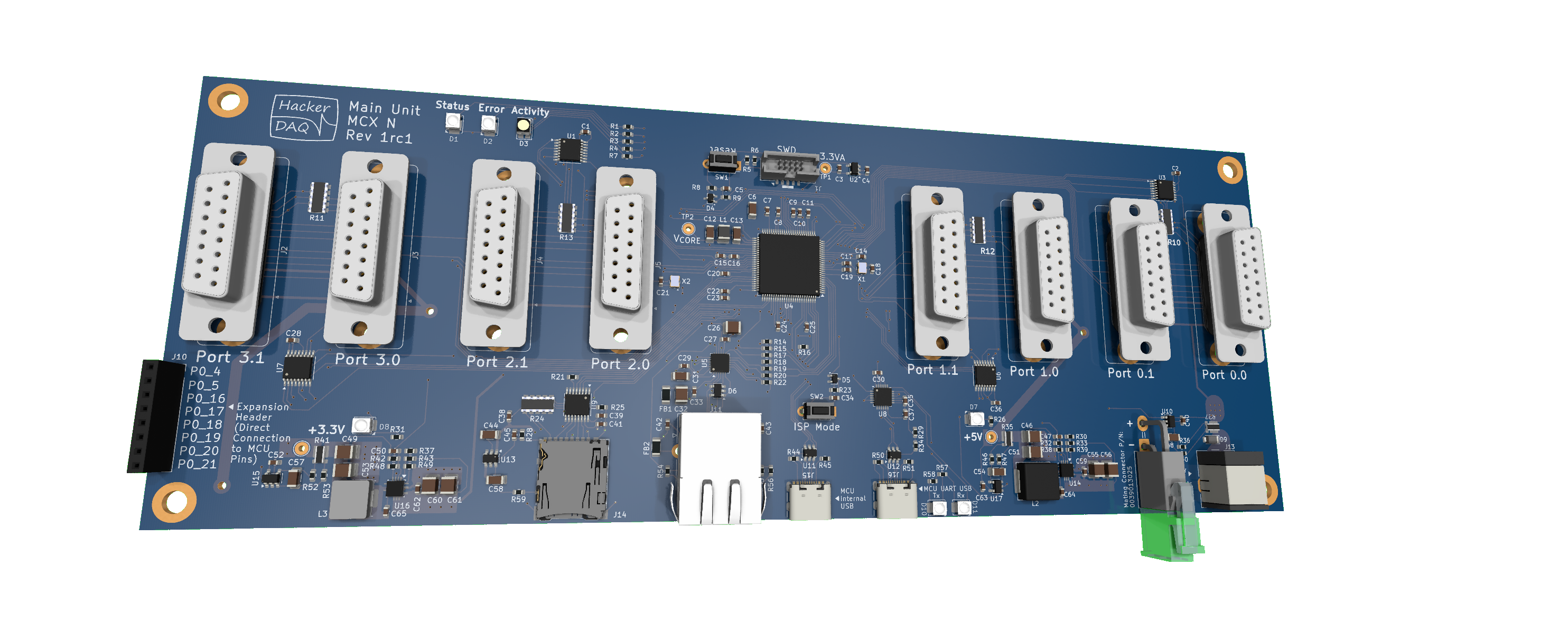
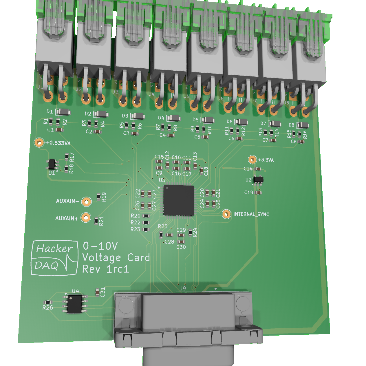
The HackerDAQ consists of a main board with a microcontroller on it and basic circuitry such as power supplies, an Ethernet port, and a MicroSD slot. The main board would have a number of connectors for cards to plug in, each of which carries power, GPIOs, and SPI bus signals.
Cards can be designed for many different applications, including digital I/O and many different types of analog sensors. The user can select only the cards they need for the application they have in mind, keeping the base cost of the system down and allowing the user to get exactly the I/O they need. The SPI bus was selected for communications with these cards as it is fast, there are a wide range of chips available that speak it, and it supports bussing together multiple chips on the card over one set of bus lines. In a lot of ways, these cards are similar to existing sensor interconnect systems like SparkFun Qwiic / Adafruit Stemma / Digilent Pmod, where you can buy various task-specific modules and connect them to a motherboard. This would just be focused more on DAQ stuff and be more industrial-grade.
In terms of software, the HackerDAQ would include firmware that would run on the board and interface with all the cards, send data to connected user interface(s), and receive and execute commands. On the PC side, there would be a basic program that can display and record data. For users who don't want to program, they can see the live data in the GUI, record it to a file, and manually control outputs. For users who are a little more comfortable with programming, they could write scripts (likely python) that would run on the host machine and be able to control the DAQ. And for users who have embedded software experience, they could write their own code that extends or replaces the firmware on the actual DAQ!
| Area | Decision | Why |
|---|---|---|
| Physical architecture | Main board + swappable cards |
|
| CPU | NXP MCX Alpha Microcontroller running Mbed OS |
|
| SPI bus topology | 2 card connectors per SPI bus, one leader card and one follower. All cards on a given bus must share the same polling rate. |
|
| Connection to host | Ethernet, potential upgrade later to add USB |
|
| Local recording | MicroSD (SPI based) |
|
| Card identification | 4kiB SPI EEPROM on the card (thinking M95320-RMN6) |
|
| Card to sensor connectors | Molex Mini-Fit |
|
| Card to main board connector | 15-pin, 2 row D-Sub (DA-15) |
|
The main unit contains a high performance MCX Alpha microcontroller with Ethernet, multiple SPI busses, a MicroSD slot, and a number of extra GPIO pins.
Both the Ethernet and the MicroSD card are available for recording data. The Ethernet is for livestreaming when you want to view, record, and process data on a PC, while the MicroSD card would be used for simple applications where you just want to record locally, and could also be configured as a backup so that data isn’t lost if the ethernet connection drops out.
The main unit takes in and regulates power for the HackerDAQ system. It has a DC input which can handle up to 8A at a variable voltage (9-24V). This voltage, referred to as Vsupply, is sent through the connectors into the cards for use as a higher voltage excitation supply when needed. High-current logic rails are provided for cards and attached devices to use -- currently 5V@8A and 3.3V@8A.
The main unit has four SPI busses. Each SPI bus provides two card ports, a "leader" port and a "follower" port. The leader and follower ports on a given bus can have different cards connected, but must operate at the same speed as SPI transactions for all cards will happen at a fixed cycle rate for the bus.
Some of the microcontroller I/O pins that are not connected to one of the SPI busses are routed to the expansion port. This will include some digital pins (with I2C/PWM/UART) and some analog pins. Advanced users who are comfortable programming embedded C++ can add write their own software that uses these pins. This allows the HackerDAQ to be used as a jumping-off point for one's own projects!
Also, SWD debug pins and reset pin are broken out to an ARM SWD debug connector, for use with a debug tool like a J-Link or MCU-Link.
The main unit would provide the following signals to each card:
Each analog card would contain the same basic DNA:
| Qty | Value | Footprint | References |
|---|---|---|---|
| 12 | 1µF | Capacitor_SMD:C_0603_1608Metric | C9, C11, C12, C13, C14, C16, C21, C22, C25, C26, C28, C30 |
| 11 | 100nF | Capacitor_SMD:C_0603_1608Metric | C5, C10, C15, C17, C18, C19, C20, C23, C24, C27, C29 |
| 8 | 0039301040 | Project Library:Molex_Mini-Fit_Jr_5569-04A2_2x02_P4.20mm_Horizontal | J1, J2, J3, J4, J5, J7, J8, J9 |
| 8 | 10.2k | Resistor_SMD:R_0603_1608Metric | R2, R4, R6, R8, R10, R12, R14, R16 |
| 8 | 1nF | Capacitor_SMD:C_0603_1608Metric | C1, C2, C3, C4, C6, C7, C8, C31 |
| 8 | 3.4k | Resistor_SMD:R_0603_1608Metric | R1, R3, R5, R7, R9, R11, R13, R15 |
| 8 | NetTie_2 | Project Library:NetTie-2_SMD_Pad0.2mm | NT1, NT2, NT3, NT4, NT5, NT6, NT7, NT8 |
| 8 | SMF11A | Diode_SMD:D_SMF | D1, D2, D3, D4, D5, D6, D7, D8 |
| 5 | 10k | Resistor_SMD:R_0603_1608Metric | R19, R20, R21, R22, R23 |
| 3 | 33 | Resistor_SMD:R_0603_1608Metric | R24, R25, R33 |
| 1 | +0.533VA | TestPoint:TestPoint_THTPad_D2.5mm_Drill1.2mm | TP1 |
| 1 | +3.3VA | TestPoint:TestPoint_THTPad_D2.5mm_Drill1.2mm | TP2 |
| 1 | 162k | Resistor_SMD:R_0603_1608Metric | R17 |
| 1 | 44.2k | Resistor_SMD:R_0603_1608Metric | R18 |
| 1 | AD7770 | Project Library:LFCSP-64-1EP_9x9mm_P0.5mm_EP5.21x5.21mm_LeadsExtended | U3 |
| 1 | AUXAIN+ | TestPoint:TestPoint_THTPad_D2.5mm_Drill1.2mm | TP5 |
| 1 | AUXAIN- | TestPoint:TestPoint_THTPad_D2.5mm_Drill1.2mm | TP3 |
| 1 | INTERNAL_SYNC | TestPoint:TestPoint_THTPad_D2.5mm_Drill1.2mm | TP4 |
| 1 | LD15S33E4GX00LF | Project Library:Amphenol_LD15S33E4GX00LF | J6 |
| 1 | M95320-RMN6 | Package_SO:SOIC-8_3.9x4.9mm_P1.27mm | U9 |
| 1 | OPA310xDBV | Package_TO_SOT_SMD:SOT-23-5 | U1 |
| 1 | TLV71333PDBV | Package_TO_SOT_SMD:SOT-23-5 | U2 |
| 1 | ~ | Project Library:HackerDAQ Logo | LG1 |
It measures 90 × 90 mm and has 2 copper layers, 1.6 mm thick.
92 parts, built around the M95320-RMN6TP, TLV71333PDBV and SMF11A. The full list of its parts is on this page, with links to each part's symbol and footprint where PCBKit's library has them.
From the multiplemonomials/HackerDAQ repository on GitHub, at the commit this page was made from: the board is hardware/Voltage Card/HackerDAQ Voltage Card.kicad_pcb and its schematic hardware/Common Sheets/5V_To_3.3V_LDO.kicad_sch. PCBKit opens the board in the browser, with nothing to install.
Its repository states no licence, so its author keeps all rights: ask multiplemonomials before reusing the design.


R-Mutura/AD_POWER_DEVICE
Highly integrated Single board Computer with RK3566


MouseBiteLabs/Super-Game-Boy-Plus
A replacement circuit board for improving the Super Game Boy, or for creating a standalone Game Boy game for the SNES.


Kiogora/esp32_lora_gateway
/ ) | | ( ( | | | | \ \| | ( ) |/ ) \ ) ) | | | || || ( (| | | | (/|)||| \))\)| || (C)2013 Semtech-Cycleo

AyushShuklaaa7/USB-C-to-I2C-Interface-FT201XS-
A compact and simple USB-C to I2C interface built using the FT201XS IC. This board is designed to provide an easy way to communicate with I2C devices directly from a computer via USB.

