2 layers47.6 × 27.3 mm

 MrKillerShaunBa/BajajPad
Made a Macropad !!!
Hackpad is an open-source printed circuit board by MrKillerShaunBa, from the MrKillerShaunBa/BajajPad repository on GitHub. It is a 2-layer board of 85.6 × 84.8 mm with 27 parts on 26 nets, routed with 133 tracks and 4 vias.
Its parts include 12 diodes, 12 switches, 1 IC and 1 connector. It belongs with the keyboards and input boards and the RP2040 boards of this library.
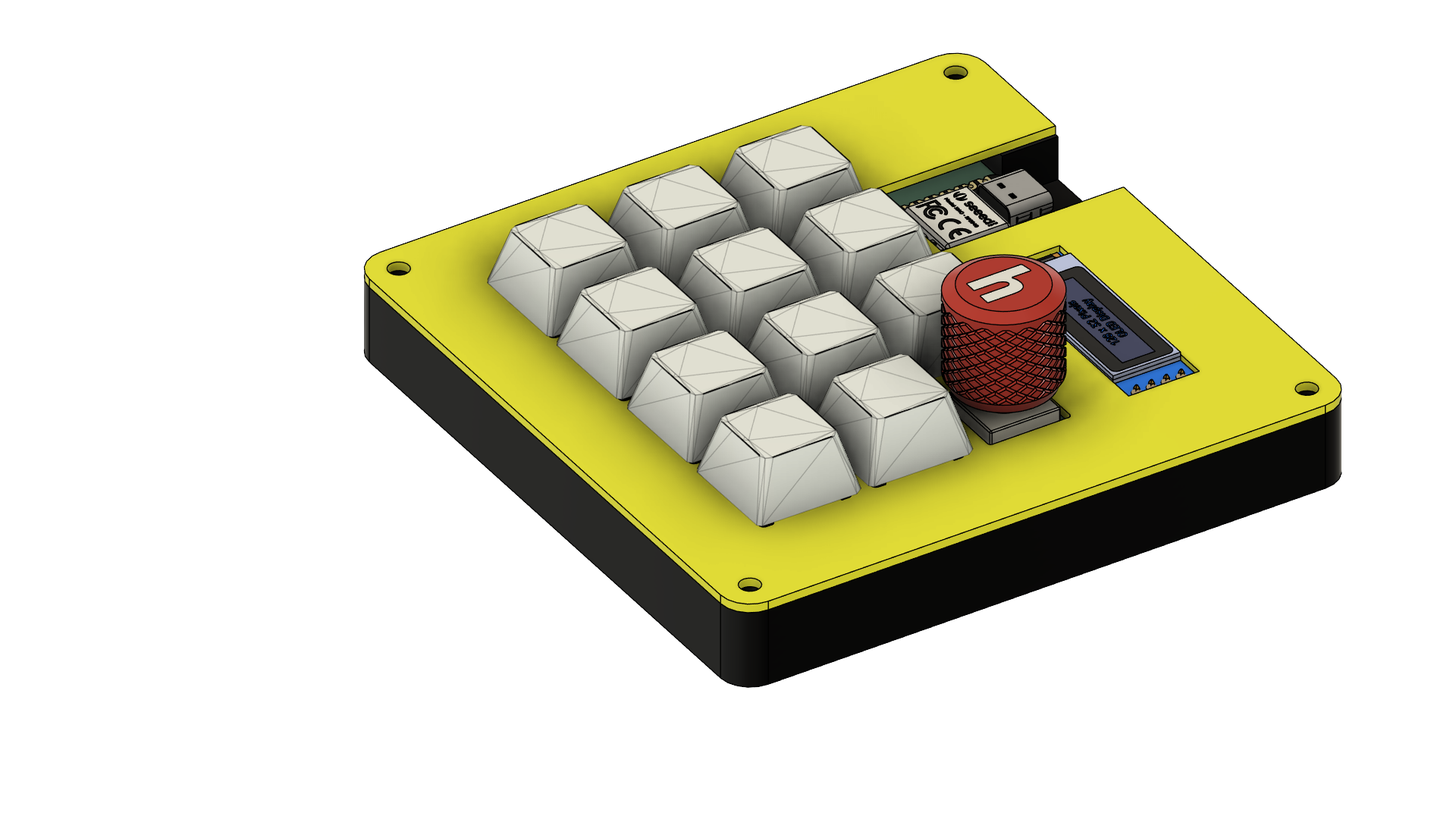 A handy macropad with a rotary encoder and an OLED display. This is created for the Hack Club HackPad V3 YSWS.
I looked at so many different projects which motivated me to try my hand at this.
I used 3D modelling and PCB software for the first time. It took a lot of time and a lot of Google searches to finally complete it. I faced a lot of problems in Fusion 360 particularly when aligning the case parts, PCB and keycaps for a test fit.
| Schematic | PCB | Case |
|---|---|---|
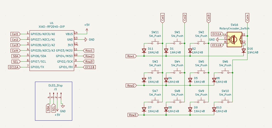 | 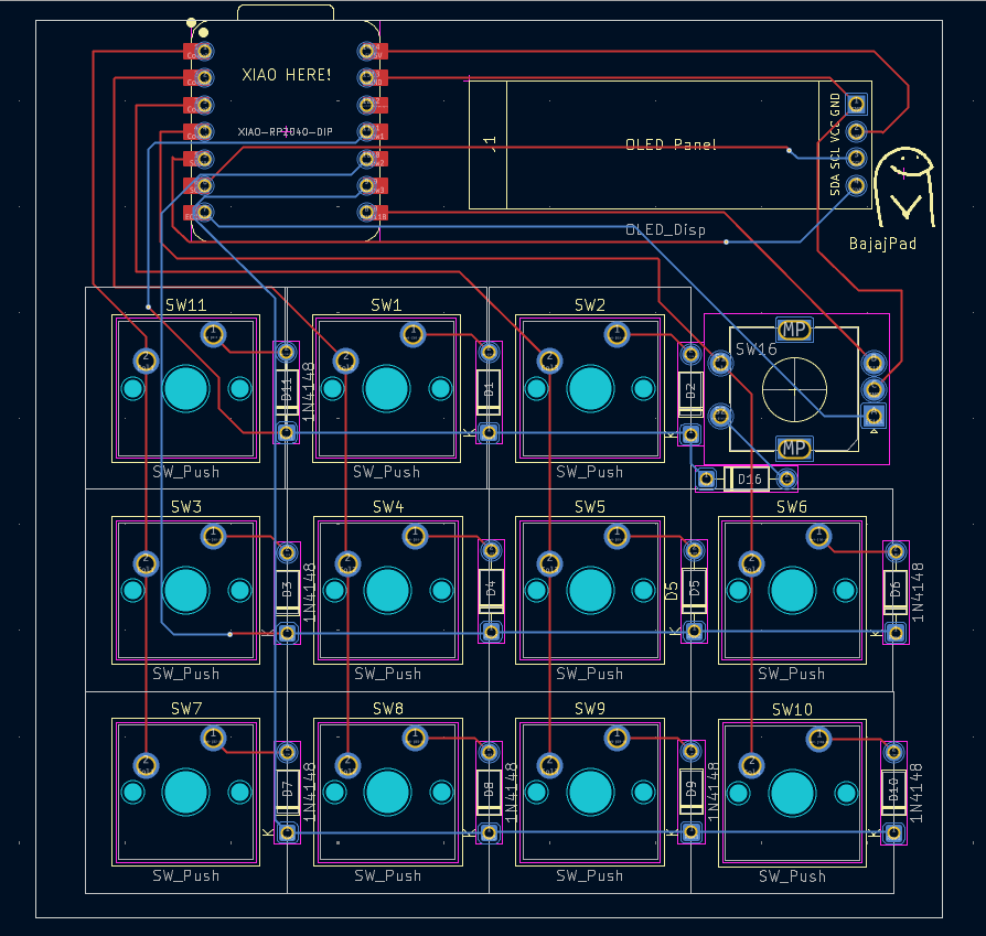 | 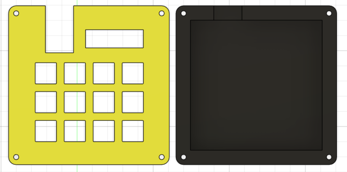 |
| Qty | Value | Footprint | References |
|---|---|---|---|
| 12 | 1N4148 | Diode_THT:D_DO-35_SOD27_P7.62mm_Horizontal | D1, D2, D3, D4, D5, D6, D7, D8, D9, D10, D11, D16 |
| 11 | SW_Push | hackpad:SW_Cherry_MX_1.00u_PCB_3D | SW1, SW2, SW3, SW4, SW5, SW6, SW7, SW8, SW9, SW10, SW11 |
| 1 | LOGO | Photo:ok | G*** |
| 1 | OLED_Disp | hackpad:SSD1306-0.91-OLED-4pin-128x32_3d | J1 |
| 1 | RotaryEncoder_Switch | hackpad:RotaryEncoder_Alps_EC11E-Switch_Vertical_H20mm_3d | SW16 |
| 1 | XIAO-RP2040-DIP | hackpad:XIAO-RP2040-DIP_3d | U1 |

hackclub/OnBoard
💡 Join 1,000 teenagers and make your first PCB with a $100 grant!


CRImier/MyKiCad
My KiCad boards. Can't be bothered uploading individually anymore, so here you go.

pjgpetecodes/pico-streamdeck
This project is an OBS Controller using a Raspberry Pi Pico and CircuitPython.

freeDSP/freeDSP-aurora
freeDSP ADAU1452 with 8 analog input, 8 analog outputs, S/P-DIF I/O, ADAT I/O, USB Audio Class2, WiFi, Bluetooth

ugcs/ddc
Drone Show Software is software designed for drone shows, allowing flight path planning as well as control of dozens of drones simultaneously in a synchronized manner.
It measures 85.6 × 84.8 mm and has 2 copper layers, 1.6 mm thick.
27 parts. The full list of its parts is on this page, with links to each part's symbol and footprint where PCBKit's library has them.
From the MrKillerShaunBa/BajajPad repository on GitHub, at the commit this page was made from: the board is PCB/hackpad.kicad_pcb and its schematic PCB/hackpad.kicad_sch. PCBKit opens the board in the browser, with nothing to install.
Its repository states no licence, so its author keeps all rights: ask MrKillerShaunBa before reusing the design.