
2 layers100 × 100 mm
BQ76pl455a
g-rahul/BQ76PL455A-EVM-Clone
This respository contains low cost design files for BQ76PL455A-EVM Clone.
255 parts5

 mrblackchris/GDB_HalfBridge
Half bridge driver using IR2104 for up to 600V DC supplies
GDB HalfBridge is an open-source printed circuit board by mrblackchris, from the mrblackchris/GDB_HalfBridge repository on GitHub. It is a 2-layer board of 43.9 × 33.5 mm with 25 parts on 23 nets, routed with 104 tracks and 11 vias.
It is built around the TBA 2-1213, IR2104PBF and MRA4007T3G-FS. Its parts include 6 connectors, 5 capacitors, 5 resistors, 4 ICs and 2 diodes. It belongs with the interfaces and adapters boards of this library.


A compact gate driver PCB for controlling an external half-bridge power stage. The design combines an IR2104 half-bridge driver, optocoupled PWM and shutdown inputs, and an onboard DC/DC converter for the gate driver supply.
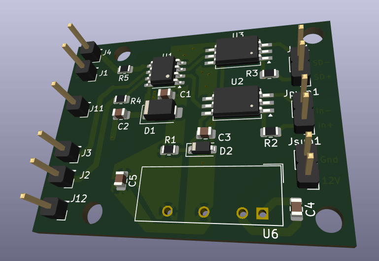
The connector names below match the schematic. Refer to the schematic for pin assignments and signal references.
| Reference | Schematic label | Purpose |
|---|---|---|
| Jsup1 | VSup | Nominal 12 V supply input |
| Jpwm1 | PWM_IN | PWM control input |
| Jsd1 | SDIN | Shutdown control input |
| J2 | GateHi | High-side gate connection |
| J3 | SourceHi | High-side source / switching-node connection |
| J4 | GateLo | Low-side gate connection |
| J1 | SourceLo | Low-side source connection |
| J12 | DrainHi | High-side drain connection |
| J11 | Temp1 | Auxiliary connection labeled Temp1 |
| File | Description |
|---|---|
| GDB_HalfBridge.kicad_pro | KiCad project |
| GDB_HalfBridge.kicad_sch | Circuit schematic |
| GDB_HalfBridge.kicad_pcb | PCB layout |
*.gbr | Exported Gerber manufacturing files |
*.drl | Plated and non-plated drill files |
| gdb_halfbridge.png | 3D board render |
Open GDB_HalfBridge.kicad_pro in KiCad to view or edit the schematic and layout. Regenerate manufacturing files after making changes to the design.
This repository documents the board design. Operating voltage, switching frequency, thermal performance, and isolation capability of the assembled board require validation for the intended application.
| Qty | Value | Footprint | References |
|---|---|---|---|
| 4 | 100n | Capacitor_SMD:C_0805_2012Metric | C1, C3, C4, C5 |
| 3 | 1k | Resistor_SMD:R_0805_2012Metric | R1, R2, R3 |
| 2 | 1 | Resistor_SMD:R_0805_2012Metric | R4, R5 |
| 2 | ACPL-P343 | Package_SO:SSO-6_6.8x4.6mm_P1.27mm_Clearance7mm | U2, U3 |
| 1 | 10u | Capacitor_SMD:C_0805_2012Metric | C2 |
| 1 | 4V7 | Diode_SMD:D_SOD-123 | D2 |
| 1 | DrainHi | Connector_PinHeader_2.54mm:PinHeader_1x01_P2.54mm_Vertical | J12 |
| 1 | GateHi | Connector_PinHeader_2.54mm:PinHeader_1x01_P2.54mm_Vertical | J2 |
| 1 | GateLo | Connector_PinHeader_2.54mm:PinHeader_1x01_P2.54mm_Vertical | J4 |
| 1 | IR2104 | Package_SO:SOIC-8_3.9x4.9mm_P1.27mm | U1 |
| 1 | MRA4007T3G | Diode_SMD:D_SMA | D1 |
| 1 | PWM_IN | Connector_PinHeader_2.54mm:PinHeader_1x02_P2.54mm_Vertical | Jpwm1 |
| 1 | SDIN | Connector_PinHeader_2.54mm:PinHeader_1x02_P2.54mm_Vertical | Jsd1 |
| 1 | SourceHi | Connector_PinHeader_2.54mm:PinHeader_1x01_P2.54mm_Vertical | J3 |
| 1 | SourceLo | Connector_PinHeader_2.54mm:PinHeader_1x01_P2.54mm_Vertical | J1 |
| 1 | TBA2-1213 | Converter_DCDC:Converter_DCDC_TRACO_TBA2-xxxx_Single_THT | U6 |
| 1 | Temp1 | Connector_PinHeader_2.54mm:PinHeader_1x01_P2.54mm_Vertical | J11 |
| 1 | VSup | Connector_PinHeader_2.54mm:PinHeader_1x02_P2.54mm_Vertical | Jsup1 |
It measures 43.9 × 33.5 mm and has 2 copper layers, 1.6 mm thick.
25 parts, built around the TBA 2-1213, IR2104PBF and MRA4007T3G-FS. The full list of its parts is on this page, with links to each part's symbol and footprint where PCBKit's library has them.
From the mrblackchris/GDB_HalfBridge repository on GitHub, at the commit this page was made from: the board is GDB_HalfBridge.kicad_pcb and its schematic GDB_HalfBridge.kicad_sch. PCBKit opens the board in the browser, with nothing to install.
Its repository states no licence, so its author keeps all rights: ask mrblackchris before reusing the design.
g-rahul/BQ76PL455A-EVM-Clone
This respository contains low cost design files for BQ76PL455A-EVM Clone.

Cyrillinux/Ardui89
Adds 8051 architecture family to the Arduino IDE : STC89C52RC, STC89C516RD+, STC15W408AS-DIP16

ilyushkin/auto_dimmer
Automatic dimmer for IKEA NYMANE (103.569.62) lamp based on AVR ATtiny13A MCU.

promesoft/KicadJE_LFO_1
Initial Analogue LFO - Mult/Mix - NAND/AND/NOT - FlipFlop - 555LFO


bostang/PCBs
My repository for documenting all PCB Projects I have done

