2 layers139.7 × 73.7 mm

 mppks/k3ng_cw1
My schematic for building the popular K3NG CW telegraph keyer
K3ng cw scheme is an open-source printed circuit board by mppks, from the mppks/k3ng_cw repository on GitHub. It is a 2-layer board of 100 × 98.4 mm with 40 parts on 45 nets, routed with 102 tracks and 0 vias.
Its parts include 13 resistors, 5 switches, 4 capacitors, 3 diodes and 3 connectors. It belongs with the AVR (ATmega, ATtiny) boards of this library.
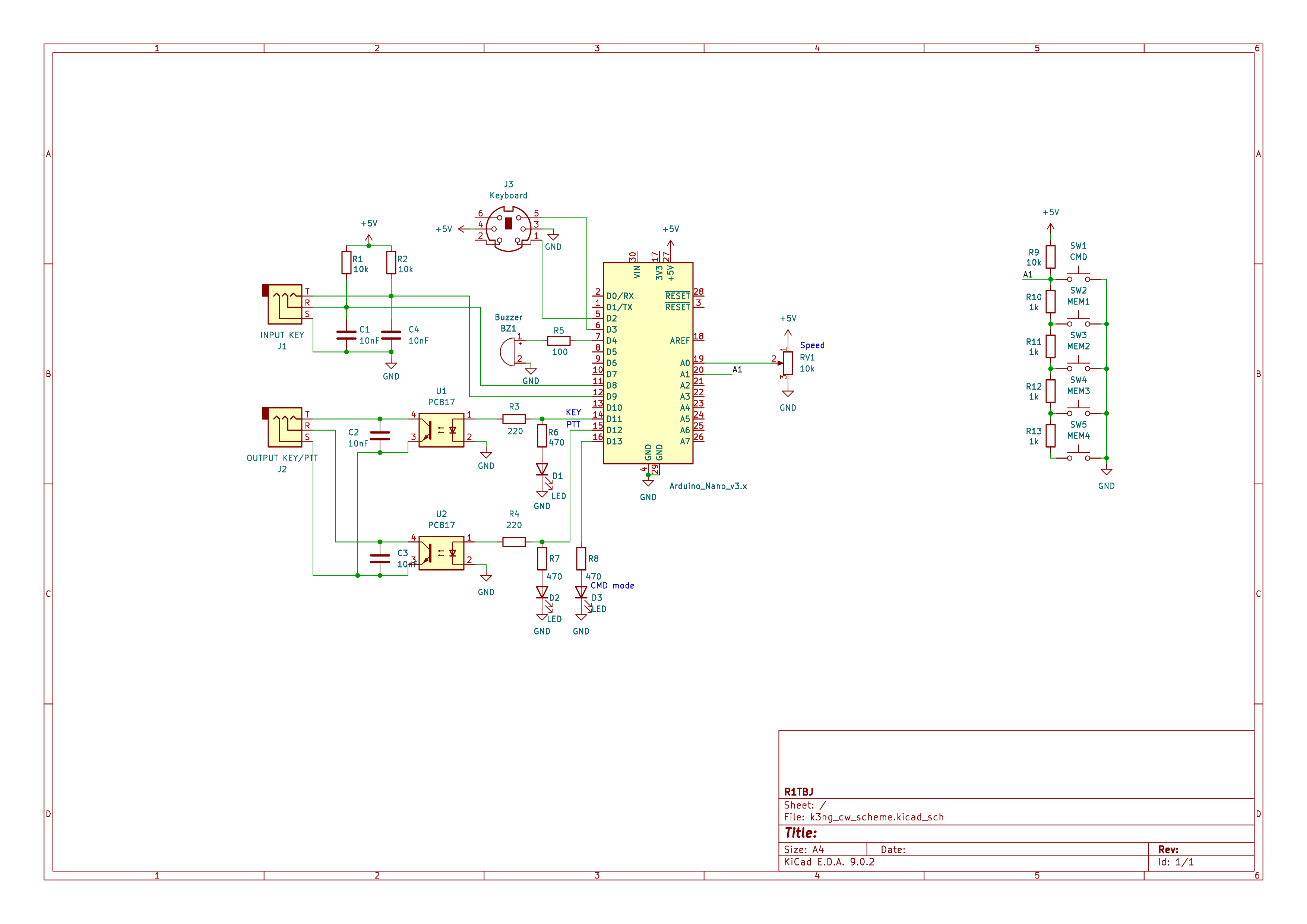
To use my keyer settings, copy the files from the r1tbj_settings directory to the original k3ng firmware directory and add the following line to the keyer_hardware.h file
#define HARDWARE_R1TBJ| Qty | Value | Footprint | References |
|---|---|---|---|
| 4 | 10nF | Capacitor_THT:C_Disc_D5.0mm_W2.5mm_P2.50mm | C1, C2, C3, C4 |
| 4 | 1k | Resistor_THT:R_Axial_DIN0207_L6.3mm_D2.5mm_P10.16mm_Horizontal | R10, R11, R12, R13 |
| 3 | 470 | Resistor_THT:R_Axial_DIN0204_L3.6mm_D1.6mm_P5.08mm_Vertical | R6, R7, R8 |
| 3 | LED | LED_THT:LED_D3.0mm | D1, D2, D3 |
| 2 | 10k | Resistor_THT:R_Axial_DIN0204_L3.6mm_D1.6mm_P5.08mm_Vertical | R1, R2 |
| 2 | 220 | Resistor_THT:R_Axial_DIN0204_L3.6mm_D1.6mm_P5.08mm_Vertical | R3, R4 |
| 2 | PC817 | Package_DIP:DIP-4_W7.62mm | U1, U2 |
| 1 | 100 | Resistor_THT:R_Axial_DIN0204_L3.6mm_D1.6mm_P5.08mm_Vertical | R5 |
| 1 | 10k | Potentiometer_THT:Potentiometer_Alpha_RD901F-40-00D_Single_Vertical | RV1 |
| 1 | 10k | Resistor_THT:R_Axial_DIN0207_L6.3mm_D2.5mm_P10.16mm_Horizontal | R9 |
| 1 | Arduino_Nano_v3.x | Module:Arduino_Nano | A1 |
| 1 | Buzzer | Buzzer_Beeper:Buzzer_12x9.5RM7.6 | BZ1 |
| 1 | CMD | Button_Switch_THT:SW_SPST_Omron_B3F-50xx | SW1 |
| 1 | INPUT KEY | Connector_Audio:Jack_3.5mm_CUI_SJ1-3525N_Horizontal | J1 |
| 1 | Keyboard | Footprints:Connector_Mini-DIN_Female_6Pin_2rows | J3 |
| 1 | MEM1 | Button_Switch_THT:SW_SPST_Omron_B3F-50xx | SW2 |
| 1 | MEM2 | Button_Switch_THT:SW_SPST_Omron_B3F-50xx | SW3 |
| 1 | MEM3 | Button_Switch_THT:SW_SPST_Omron_B3F-50xx | SW4 |
| 1 | MEM4 | Button_Switch_THT:SW_SPST_Omron_B3F-50xx | SW5 |
| 1 | OUTPUT KEY/PTT | Connector_Audio:Jack_3.5mm_CUI_SJ1-3525N_Horizontal | J2 |
The 33 most common of 40 parts.

hackclub/OnBoard
💡 Join 1,000 teenagers and make your first PCB with a $100 grant!

Chrismettal/EleLab_v2
Cheap DIY lab system for hobbyists and the tinkering folk

Chrismettal/flipper-zero-backpacks
Backpack-style addon boards for the Flipper Zero!


ohmtech-rdi/eurorack-blocks
Software to Hardware Prototyping for Eurorack using C++, Max/Gen~ or Faust

It measures 100 × 98.4 mm and has 2 copper layers, 1.6 mm thick.
40 parts. The full list of its parts is on this page, with links to each part's symbol and footprint where PCBKit's library has them.
From the mppks/k3ng_cw repository on GitHub, at the commit this page was made from: the board is k3ng_cw_scheme/k3ng_cw_scheme.kicad_pcb and its schematic k3ng_cw_scheme/k3ng_cw_scheme.kicad_sch. PCBKit opens the board in the browser, with nothing to install.
Its repository states no licence, so its author keeps all rights: ask mppks before reusing the design.