2 layers103 × 30.5 mm

 moucha19/DS4-DB-Type-C8
USB-C daughterboard for DualShock 4 controller
Jds-040 is an open-source printed circuit board by moucha19, from the moucha19/DS4-DB-Type-C repository on GitHub, published under the CERN-OHL-W-2.0 licence. It is a 2-layer board of 18.1 × 21.5 mm with 9 parts on 15 nets, routed with 73 tracks and 28 vias.
Its parts include 2 resistors, 2 connectors, 1 capacitor, 1 diode and 1 fuse.
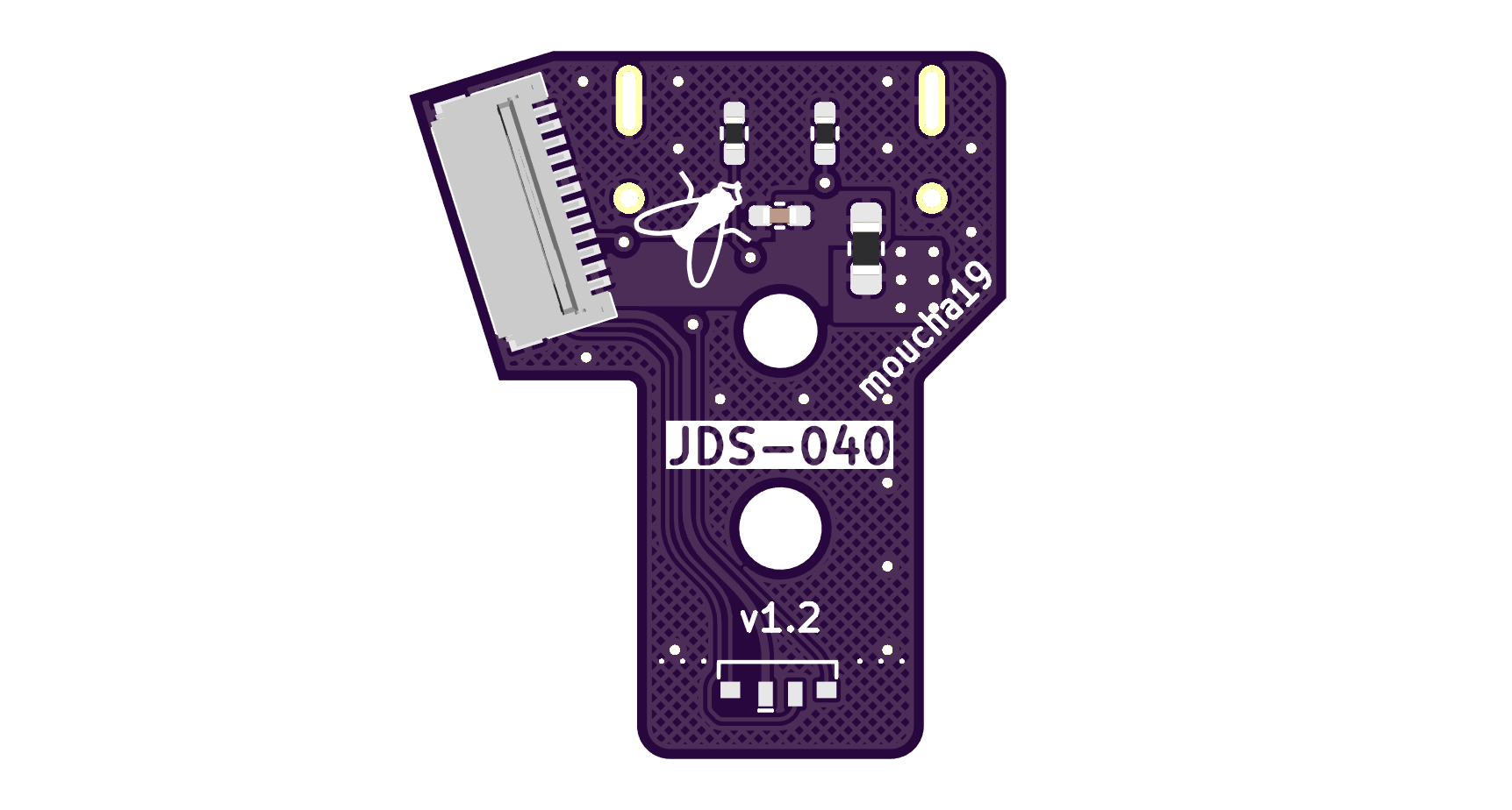
You can find the archive with Gerber files in the releases section.
When ordering, you must choose a 1.2 mm PCB thickness!
| Designator | Footprint | LCSC |
|---|---|---|
| C1 | 10nF SMD 0402 Capacitor | C15195 |
| D1 | LED RGB Foshan FM-3510RGBA-SG | C727903 |
| F1 | 6V 750mA SMD 0603 Fuse | C207016 |
| FL1 | TDK MCZ1210DH Common mode filter | C383353 |
| J1 | USB-C Receptacle GT-USB-7025 | C963213 |
| J2 | JUSHUO AFC42-S12FMA-1H or MOLEX 5034801200 | C466532 or C587969 |
| R1,R2 | 5.1k SMD 0402 Resistor | C105872 |
This is a very small and finicky board. I made no optimizations for the SMT assembly, because you need to solder fine pitch connectors and components on both sides of the board. It may still be a viable option if you can get assembly for both sides, but since the part count is very low, you can also manage the assembly on your own if you have a right equipment.
Hot air gun is very handy, especially for soldering of the USB-C and FPC connectors. In my opinion, the easiest method is to tin all of the pads first and then simply position the connectors under the hot air. Rest of the components is manageable with a reasonably fine soldering iron.
I would highly recommend you to watch instruction video from Marius Heier, on YouTube. He created it as a guide for mounting of his own USB-C DualShock 4 mods and his advice on how to enlarge the charging port hole is excellent. Definitely start from the inside first. It might be tempting to grab a Dremel but it's safer to proceed just like in the video, manually with a small file.
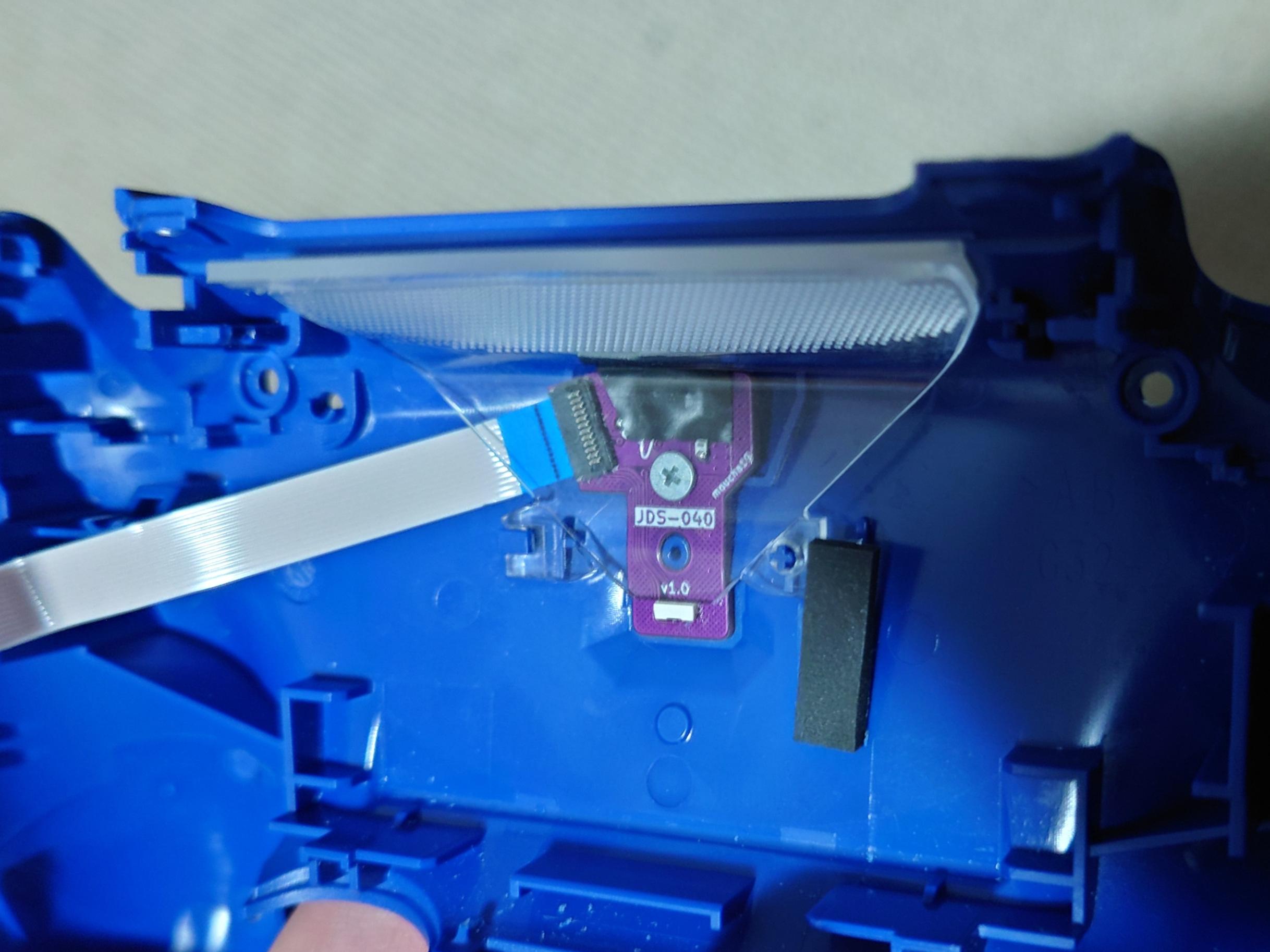
Some additional advice that I can give after going through the process is to take it slow once you start making the charging port hole larger. You absolutely MUST take away some material both from top and bottom of the hole. One mistake I did was that I focused on the bottom first and then went a little overboard. I should've proceeded symmetricaly because the top also had to be filed down. You can find detailed photos below so you have some idea where roughly to stop. The USB symbol is a good reference.
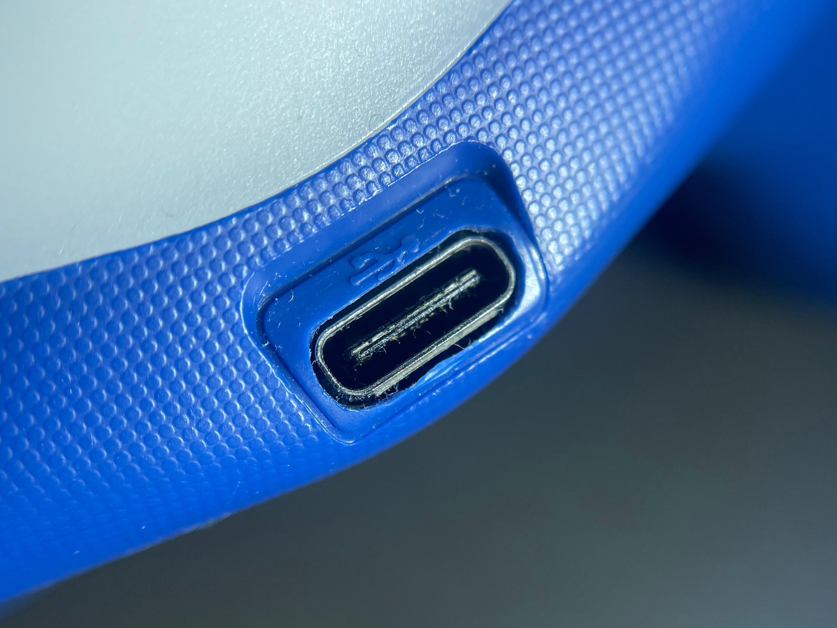
The toughest challenge when designing the board was deciding where exactly to position the charging port. I did not want it to protrude but on the other hand, I did not want to bury it too much, with a visible gap between the plastic and the edge of the connector. In the end, this is how it looks and I'm quite satisfied with the result. The bottom of the connector is visible a little bit, but the top edge is in the ideal position. Anyways, here is a detail so you easily decide to modify the board and shift the connector in either direction based on your preference. The protrusion is roughly 0.4 mm.
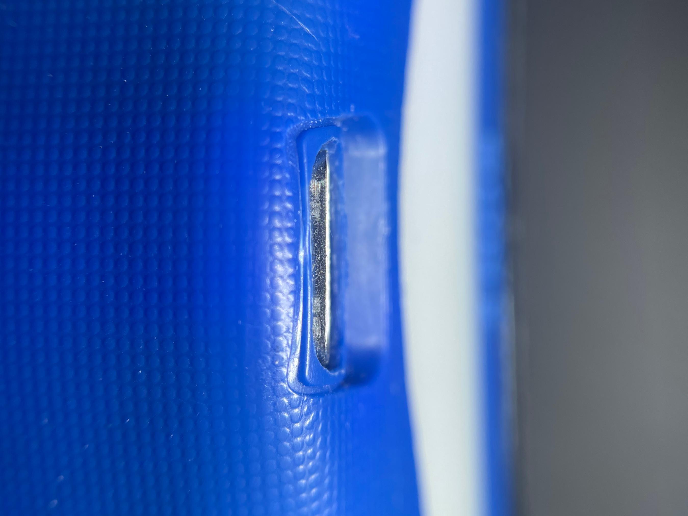
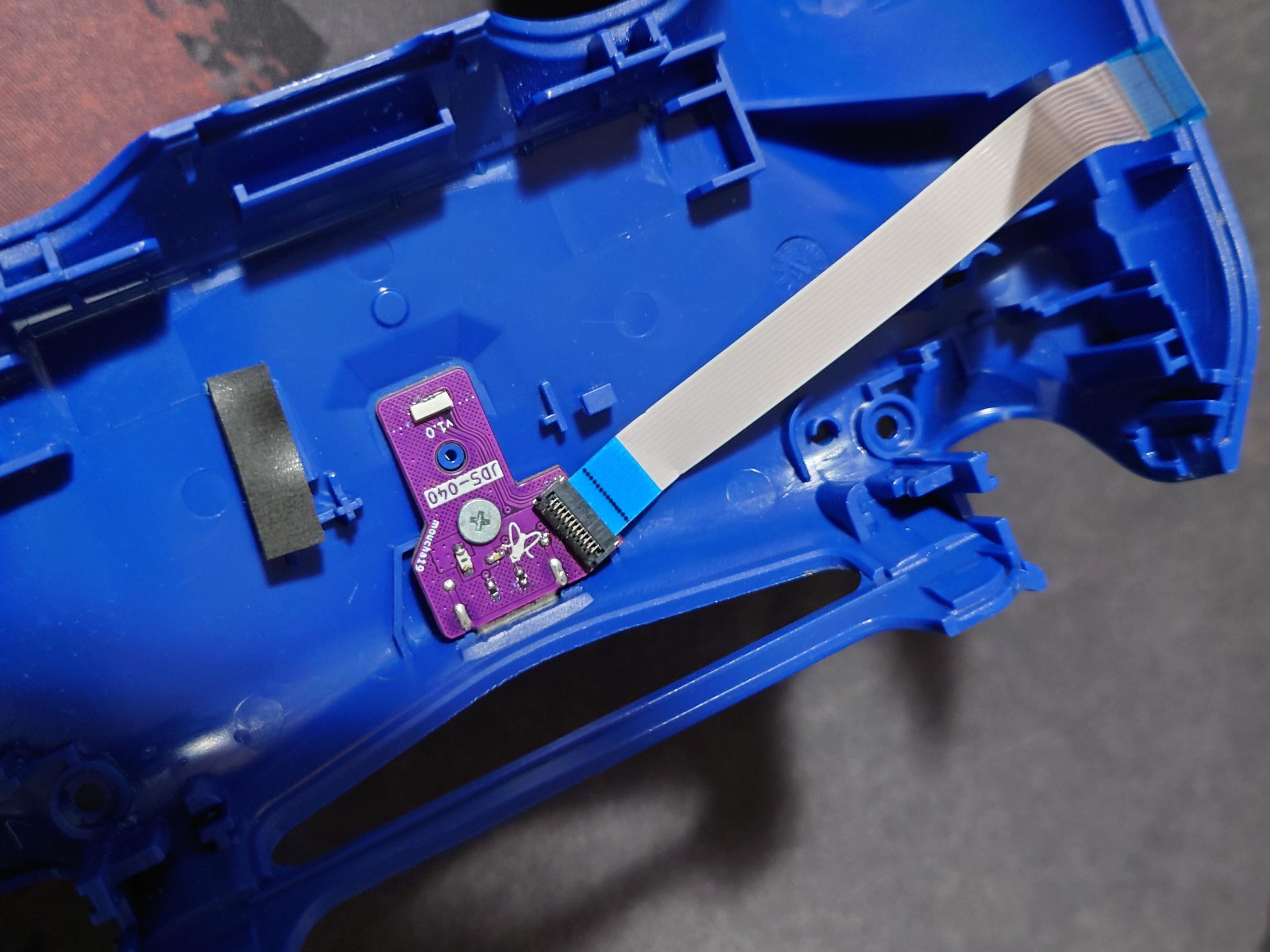
Rest of the process is very easy though and the board should fit snugly. When it comes to the light output, the LED I chose performs as well as the original and I was not able to tell the difference.
| Qty | Value | Footprint | References |
|---|---|---|---|
| 2 | 5.1k | Resistor_SMD:R_0402_1005Metric_Pad0.72x0.64mm_HandSolder | R1, R2 |
| 1 | 10nF | Capacitor_SMD:C_0402_1005Metric_Pad0.74x0.62mm_HandSolder | C1 |
| 1 | 750 mA | Fuse:Fuse_0603_1608Metric_Pad1.05x0.95mm_HandSolder | F1 |
| 1 | FPC_01x12 | Moucha_Connectors:FPC_CompactUniversal_12P | J2 |
| 1 | Filter_EMI_CommonMode | Moucha_Primitives:L_CommonMode_TDK_MCZ1210DH | FL1 |
| 1 | LED_ARGB | Moucha_Primitives:LED_RGB_Foshan-FM-3510RGBA-SG | D1 |
| 1 | USB_C_Receptacle_USB2.0 | Moucha_Connectors:USBC_Receptacle_GT-USB-7025 | J1 |
The 8 most common of 9 parts.
It measures 18.1 × 21.5 mm and has 2 copper layers, 1.2 mm thick.
9 parts. The full list of its parts is on this page, with links to each part's symbol and footprint where PCBKit's library has them.
From the moucha19/DS4-DB-Type-C repository on GitHub, at the commit this page was made from: the board is pcb/jds-040/jds-040.kicad_pcb and its schematic pcb/jds-040/jds-040.kicad_sch. PCBKit opens the board in the browser, with nothing to install.
Its repository publishes it under the CERN-OHL-W-2.0 licence: you may reuse it on that licence's terms (keep the author's notice, and for a copyleft licence share your changes alike).


FrameworkComputer/ExpansionCards
Reference designs and documentation to create Expansion Cards for the Framework Laptop

VoronDesign/Voron-Hardware
Cool Hardware designed by the Voron Design group

hackclub/OnBoard
💡 Join 1,000 teenagers and make your first PCB with a $100 grant!


adamws/kicad-kbplacer
KiCad plugin for automatic keyboard's key placement and routing