
2 layers70 × 44 mm
Thermo bench carrier
mojealterego/FENG-LABORATORY
This folder contains native KiCad schematic/net-assigned PCB for an LTC3108 active power breakout, not a finalized complete industrial IoT device.
5 parts
 mojealterego/FENG-LABORATORY
This folder contains native KiCad schematic/net-assigned PCB for an LTC3108 active power breakout, not a finalized complete industrial IoT device.
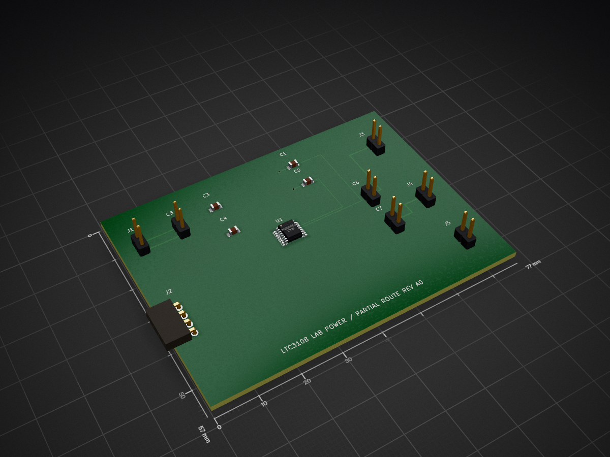
Ltc3108 power breakout is an open-source printed circuit board by mojealterego, from the mojealterego/FENG-LABORATORY repository on GitHub. It is a 2-layer board of 77 × 57 mm with 13 parts on 12 nets, routed with 33 tracks and 2 vias.
It is built around the LTC3108EGN#PBF. Its parts include 7 capacitors, 5 connectors and 1 IC. It belongs with the interfaces and adapters boards of this library.
This folder contains native KiCad schematic/net-assigned PCB for an LTC3108 active power breakout, not a finalized complete industrial IoT device. The PCB has placed parts, assigned nets, and two explicitly routed charge-pump connections (C1.2→U1.13, C2.2→U1.14); the remainder is still UNROUTED. Real KiCad 10 automated ERC/DRC has been RUN, but blocking warnings and unconnected copper remain; there is no passed manufacturing signoff, mechanical clearance/assembly validation, or hot/cold-start test. Do NOT send to PCB fabrication as is.
The design uses the LTC3108EGN 16-pin SSOP package and an external transformer for ease of bench swapping. Pin numbering matches the manufacturer GN16 top-view drawing (Rev D). Manufacturer typical application: https://www.analog.com/media/en/technical-documentation/data-sheets/3108fc.pdf.
J1 TEG source -> C5 reservoir + primary of external 1:100 transformer (J2 primary TEG_P to SW). Secondary ground/Sec_HI -> C1 1nF and C2 330pF -> LTC3108's C1/C2 charge pump. VS1=VAUX and VS2=GND selects 3.3V VOUT. C3 1uF VAUX, C4 2.2uF VLDO. J3 exposes VOUT with C6 470uF. J4 exposes 5V VSTORE for an external 0.1F / 6.3V energy reservoir (C7 DNP). J5 exposes PGD for a high-impedance diagnostic probe. VOUT2_EN tied to GND, VOUT2 unused.
Critical: J2 four-pin 2.54mm transformer breakout does not correspond to the transformer manufacturer's surface-mount pad numbering. Confirm coil polarity/pinout and orientation on the real LPR6235 before assembly; no transformer is soldered on this PCB.
| IC pin | Function | Circuit net |
|---|---|---|
| 1, 8, 9, 16 | GND | GND |
| 2 | VAUX | VAUX |
| 3 | VSTORE | VSTORE |
| 4 | VOUT | VOUT |
| 5 | VOUT2 | NC_VOUT2 / unconnected |
| 6 | VLDO | VLDO |
| 7 | PGD | PGD |
| 10 | VS2 | GND |
| 11 | VS1 | VAUX |
| 12 | VOUT2_EN | GND |
| 13 | C1 | PMIC_C1 |
| 14 | C2 | PMIC_C2 |
| 15 | SW | SW |
The local ThermoActive.pretty/ directory and fp-lib-table resolve the custom SMD/TH footprints used in the schematic. They are engineering placeholders, not manufacturer-validated land patterns. In particular, RadialCap stands for an unselected 2.54mm-pitch THT cap and can be dangerous if a larger diameter, different polarity, clearance or thermal derating is required. The SSOP16 land-pattern is provisional and must be compared with Analog Devices GN16 recommended solder pattern before release.
The manufacturer-reference capacitor-to-LTC3108 nets PMIC_C1 and PMIC_C2 have now been laid on F.Cu at 0.20 mm nominal width. The real KiCad 10.0.6 DRC diagnostics 37960523837 report 28 unconnected pads remaining, down from 30, and 13 existing footprint-library mismatch warnings. There were no new inter-track violations reported for the two routed nets. These are preliminary reference-board traces, not an undisclosed novel circuit. Transformer pin order, capacitor land-patterns, ESR, clearance, and all other wiring remain HOLD; the board shall not be manufactured or attached to live heating infrastructure without independent electrical/DFM validation.
hardware/cad_gate.py interprets KiCad textual DRC to machine-readable HOLD / ENGINEERING_REVIEW_REQUIRED. Even a hypothetical zero-violation DRC result never sets fabrication_authorized to true — a human review is mandatory.
The open C6 = 470 µF at VOUT 3.3 V is not sufficient as the sole storage capacitor for the illustrative 87 mA / 200 ms STM32WLE transmit pulse even under the optimistic constant LTC3108 VOUT current assumption. A charge/ESR first-order model suggests at least 13.1 mF for the specified illustrative pulse and minimum voltage, before derating and protection margins. This number is NOT a production capacitor selection or a validated performance value. VSTORE (nominally around 5 V) must never be directly connected to STM32WLE VDD. Independent current transient measurement and a suitable qualified power architecture remain prerequisites.
See reproducible power-integrity analysis and python -m thermo_iot.harvester_rail. Engineering status remains HOLD even if routing progress reduces unconnected pads.
| Qty | Value | Footprint | References |
|---|---|---|---|
| 1 | 0u1_VSTORE_EXTERNAL_DNP | ThermoActive:RadialCap | C7 |
| 1 | 1nF_C1 | ThermoActive:Cap0805 | C1 |
| 1 | 1uF_VAUX | ThermoActive:Cap0805 | C3 |
| 1 | 220uF_TEG | ThermoActive:RadialCap | C5 |
| 1 | 2u2_VLDO | ThermoActive:Cap0805 | C4 |
| 1 | 330pF_C2 | ThermoActive:Cap0805 | C2 |
| 1 | 470uF_VOUT_6V3 | ThermoActive:RadialCap | C6 |
| 1 | EXTERNAL_VSTORE_SUPERCAP_6V3 | ThermoActive:Header1x2 | J4 |
| 1 | External_LPR6235_752SML | ThermoActive:Header1x4 | J2 |
| 1 | LTC3108EGN | ThermoActive:SSOP16_P0635 | U1 |
| 1 | OUT_3V3_LAB | ThermoActive:Header1x2 | J3 |
| 1 | PGOOD_MONITOR | ThermoActive:Header1x2 | J5 |
| 1 | TEG | ThermoActive:Header1x2 | J1 |
mojealterego/FENG-LABORATORY
This folder contains native KiCad schematic/net-assigned PCB for an LTC3108 active power breakout, not a finalized complete industrial IoT device.


samyk/magspoof
A portable device that can spoof/emulate any magnetic stripe, credit card or hotel card "wirelessly", even on standard magstripe (non-NFC/RFID) readers.

fossasia/pslab-scripts
Pocket Science Lab - Scripts for Sensor Experiments


willem-pennings/balancing-cube
A cube that balances itself in a corner or edge using reaction wheels

VoronDesign/Voron-Hardware
Cool Hardware designed by the Voron Design group

hoglet67/RGBtoHDMI
Bare-metal Raspberry Pi project that provides pixel-perfect sampling of Retro Computer RGB/YUV video and conversion to HDMI
It measures 77 × 57 mm and has 2 copper layers, 1.6 mm thick.
13 parts, built around the LTC3108EGN#PBF. The full list of its parts is on this page, with links to each part's symbol and footprint where PCBKit's library has them.
From the mojealterego/FENG-LABORATORY repository on GitHub, at the commit this page was made from: the board is hardware/active_power/ltc3108_power_breakout.kicad_pcb and its schematic hardware/active_power/ltc3108_power_breakout.kicad_sch. PCBKit opens the board in the browser, with nothing to install.
Its repository states no licence, so its author keeps all rights: ask mojealterego before reusing the design.