2 layers75 × 55 mm

 MitchiLaser/MAXwel1
Cheap DIY FPGA development board
MAXwel is an open-source printed circuit board by MitchiLaser, from the MitchiLaser/MAXwel repository on GitHub, published under the GPL-2.0 licence. It is a 2-layer board of 78.7 × 85.7 mm with 156 parts on 176 nets, routed with 921 tracks and 352 vias.
It is built around the EPM240T100C3 and AMS1117-3.3. Its parts include 89 resistors, 25 capacitors, 17 diodes, 13 switches and 6 ICs. It belongs with the fPGA and programmable logic and microcontroller boards boards and the FPGA and CPLD boards of this library.


MAX ii Workbench for Education and Learning - MAXwel
MAXwel is a cheap and simple FPGA development board made for educational purposes. It is based in a low-cost Altera MAX ii Chip (EPM240), containing 240 logic elements, 8Kbits of RAM and 32Kbits of flash memory. The board is equipped with 8 switches, 4 push-buttons, 16 LEDs (divided into rows A and B of 8 LEDs each) and four 7-segment displays. It also contains a 50MHz oscillator and a 14,7456 MHz oscillator as a clock source. The board is programmed through a USB Blaster JTAG interface with the pin-header located on the board.
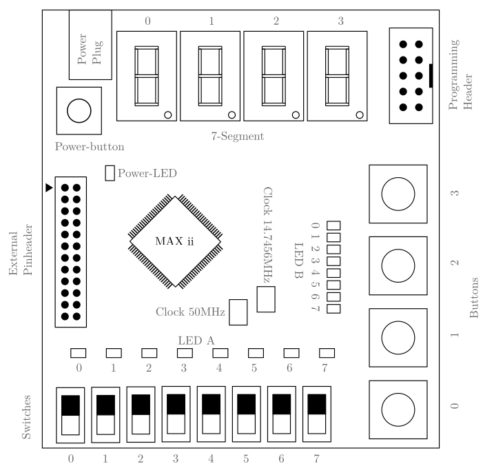
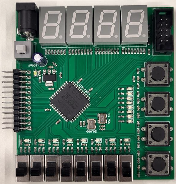
All schematics and PCB files are available in the hardware directory.
The user documentation is available in the docs directory and on the landing page.
A template for an empty VHDL project with correct pin assignments is available in the template directory.
The directory also contains a template for a schematic based circuit design.
All templates are intended to be used with the Quartus software from Intel.
There are also some features for hardcore enthusiasts.
My university uses this FPGA board for a students lab course. There is a directory containing the reference designs for the lab course exercises. The lab course exercises require the students to draw schematic diagrams in the Quartus software within a predefined template file. The Quartus software only offers the logic symbols in the US style within the schematic editor. This directory also offers EU style symbols for the project symbol library of the Quartus software.
This project is currently under heavy development.
The Overlay is an open FPGA architecture for open tools and user designs that is intended to run on the MAX ii chip, in essence an "FPGA on a FPGA". The main goal of the Overlay is to provide a simple and easy to use platform for learning and experimenting with FPGA synthesis technology. Once the overlay is synthesizes and loaded into the MAX ii chip, it will be possible to load user designs into the overlay, without the need to re-synthesize the overlay itself. This allows for a high level of flexibility and experimentation, as well as a way to learn about FPGA synthesis and design without the need for the closed source tools from the FPGA manufacturer. Emulating an FPGA inside an FPGA takes up a lot of resources. Therefore the Overlay is not made for practical use cases outside of learning and experimentation.
| Qty | Value | Footprint | References |
|---|---|---|---|
| 41 | 10K | Resistor_SMD:R_0603_1608Metric_Pad0.98x0.95mm_HandSolder | R1, R2, R3, R4, R5, R30, R31, R32, R33, R43, R46, R49, R51, R52, R53, R54 +25 |
| 32 | 470 | Resistor_SMD:R_0603_1608Metric_Pad0.98x0.95mm_HandSolder | R10, R11, R12, R13, R14, R15, R16, R17, R18, R19, R20, R21, R22, R23, R24, R25 +16 |
| 17 | LED | LED_SMD:LED_0805_2012Metric_Pad1.15x1.40mm_HandSolder | D1, D2, D3, D4, D5, D6, D7, D8, D10, D11, D12, D13, D14, D15, D16, D17 +1 |
| 16 | 1K | Resistor_SMD:R_0603_1608Metric_Pad0.98x0.95mm_HandSolder | R42, R44, R45, R47, R48, R50, R60, R61, R64, R68, R69, R70, R78, R79, R80, R81 |
| 12 | 20n | Capacitor_SMD:C_0603_1608Metric_Pad1.08x0.95mm_HandSolder | C3, C9, C13, C14, C15, C16, C17, C18, C20, C21, C22, C23 |
| 11 | 100n | Capacitor_SMD:C_0603_1608Metric_Pad1.08x0.95mm_HandSolder | C1, C2, C4, C5, C6, C7, C8, C10, C11, C12, C24 |
| 8 | SW_Wuerth_450301014042 | Library:SW_Slide_SPDT_Straight_12.8mm_6.9mm | SW5, SW6, SW7, SW8, SW10, SW11, SW12, SW13 |
| 4 | D168K | Display_7Segment:D1X8K | U1, U2, U3, U4 |
| 4 | SW_Push_Dual | Library:SW_PUSH-12mm | SW1, SW2, SW3, SW4 |
| 1 | 100µF | Capacitor_THT:CP_Radial_D5.0mm_P2.00mm | C19 |
| 1 | 14.756 | Oscillator:Oscillator_SMD_EuroQuartz_XO53-4Pin_5.0x3.2mm_HandSoldering | X2 |
| 1 | 47n | Capacitor_SMD:C_0603_1608Metric_Pad1.08x0.95mm_HandSolder | C25 |
| 1 | 50.000 | Oscillator:Oscillator_SMD_EuroQuartz_XO53-4Pin_5.0x3.2mm_HandSoldering | X1 |
| 1 | AMS1117-3.3 | Package_TO_SOT_SMD:SOT-223-3_TabPin2 | U6 |
| 1 | Barrel_Jack_Switch_Pin3Ring | Connector_BarrelJack:BarrelJack_Horizontal | J3 |
| 1 | Conn_02x05_Odd_Even | Connector_IDC:IDC-Header_2x05_P2.54mm_Vertical | J1 |
| 1 | Conn_02x12_Counter_Clockwise | Connector_PinHeader_2.54mm:PinHeader_2x12_P2.54mm_Horizontal | J2 |
| 1 | EPM240T100 | Package_QFP:TQFP-100_14x14mm_P0.5mm | U5 |
| 1 | LOGO | Library:qr_code | G*** |
| 1 | SW_Push_DPDT | Button_Switch_THT:SW_Push_2P2T_Toggle_CK_PVA2OAH5xxxxxxV2 | SW9 |
It measures 78.7 × 85.7 mm and has 2 copper layers, 1.6 mm thick.
156 parts, built around the EPM240T100C3 and AMS1117-3.3. The full list of its parts is on this page, with links to each part's symbol and footprint where PCBKit's library has them.
From the MitchiLaser/MAXwel repository on GitHub, at the commit this page was made from: the board is hardware/MAXwel.kicad_pcb and its schematic hardware/MAXwel.kicad_sch. PCBKit opens the board in the browser, with nothing to install.
Its repository publishes it under the GPL-2.0 licence: you may reuse it on that licence's terms (keep the author's notice, and for a copyleft licence share your changes alike).

RBSC/Daewoo_CPC400_Upgrade
Upgrading Daewoo CPC-400/400S into MSX2/MSX2+


RWeick/REF1329-N64-Gameshark-Clone
This implements the original LZ9FC17 GAL on an Altera EPM240. It fully supports all functionality to include: parallel port, 7 segment display, and the GS button

mtabini/G76-Mini
An inexpensive VGA circuit designed specifically for homebrew 8-bit computers

arleybls/divtiesus-acer
Custom 2-layer PCB re-layout of DivTIESUS — a DivMMC SD card interface for the ZX Spectrum, with the upstream CPLD firmware unchanged.