2 layers320.9 × 84.4 mm
 Mineinjava/anchorkeeb
split mechanical keyboard
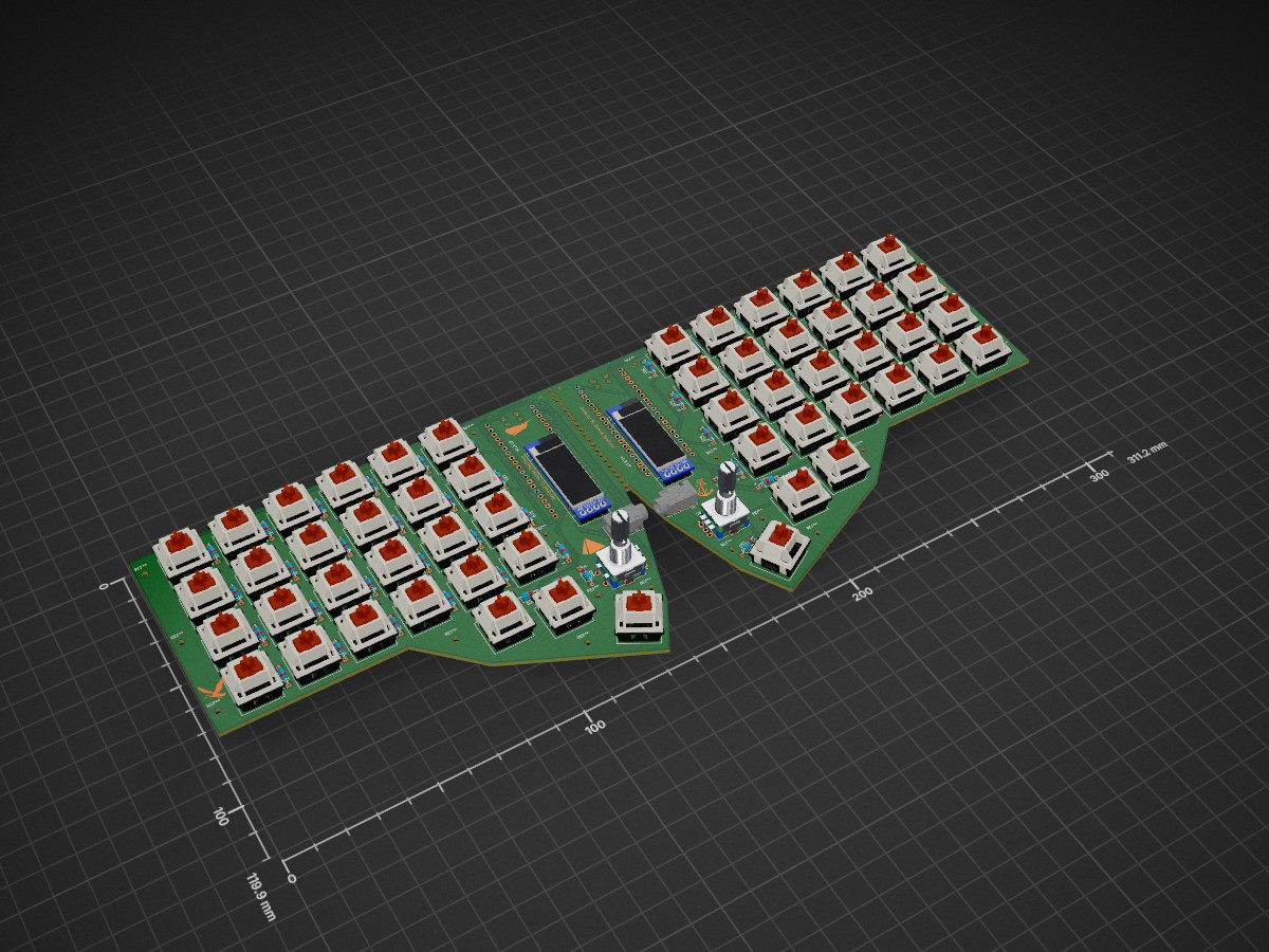
Hackboard is an open-source printed circuit board by Mineinjava, from the Mineinjava/anchorkeeb repository on GitHub. It is a 2-layer board of 311.2 × 119.9 mm with 162 parts on 138 nets, routed with 609 tracks and 13 vias.
Its parts include 56 diodes, 56 switches, 4 connectors and 2 ICs. It belongs with the keyboards and input boards and the RP2040 boards of this library.
Split mechanical keyboard. Ortholinear layout. One display, one encoder, 4x6 + 3 keys per half.
I like the look of a PCB with a lot of visible traces. To achieve this, I left the PCB exposed through the case and routed all the traces in beautiful strips where they can be seen. This took a long time to route.
Produced as part of Hack Club's Hackpad v2 project.
| Qty | Value | Footprint | References |
|---|---|---|---|
| 56 | 1N914 | Diode_THT:D_DO-35_SOD27_P7.62mm_Horizontal | D1, D2, D10, D11, D12, D13, D14, D15, D16, D17, D18, D19, D20, D21, D22, D23 +40 |
| 54 | SW_Push_45deg | Button_Switch_Keyboard:SW_Cherry_MX_1.00u_PCB | SW1, SW2, SW10, SW11, SW12, SW13, SW14, SW15, SW16, SW17, SW18, SW19, SW20, SW21, SW22, SW23 +38 |
| 6 | LOGO | LOGO | G***, G***, G***, G***, G***, G*** |
| 2 | AudioJack4 | Connector_Audio:Jack_3.5mm_PJ320E_Horizontal | J1, J2 |
| 2 | Conn_01x04_Socket | oled:SSD1306-0.91-OLED-4pin-128x32 | J3, J4 |
| 2 | Pico | MCU_RaspberryPi_and_Boards:RPi_Pico_SMD_TH | U1, U2 |
| 2 | RotaryEncoder_Switch | Rotary_Encoder:RotaryEncoder_Alps_EC11E-Switch_Vertical_H20mm | SW28, SW56 |
The 124 most common of 162 parts.
It measures 311.2 × 119.9 mm and has 2 copper layers, 1.6 mm thick.
162 parts. The full list of its parts is on this page, with links to each part's symbol and footprint where PCBKit's library has them.
From the Mineinjava/anchorkeeb repository on GitHub, at the commit this page was made from: the board is anchorkeeb/pcb/Hackboard.kicad_pcb and its schematic anchorkeeb/pcb/Hackboard.kicad_sch. PCBKit opens the board in the browser, with nothing to install.
Its repository states no licence, so its author keeps all rights: ask Mineinjava before reusing the design.

themaxbang/MRIYA
MRIYA is a 42-key column-staggered split keyboard based on the Corne Cherry v.3.0.1

keebio/quefrency-rev1-pcb
Quefrency Rev. 1 Keyboard PCB =============================

kelvinhall05/Southpaw75
Design files and assembly guide for the Southpaw75 keyboard.


bnepethomas/bne-arduino-flight-simulator-interfaces
Automatically exported from code.google.com/p/bne-arduino-flight-simulator-interfaces

Testbild-synth/super-sweet-16
Deluxe 16-step knob-per-function sequencer Module for eurorack