Skip to the content
PCBKitNew board
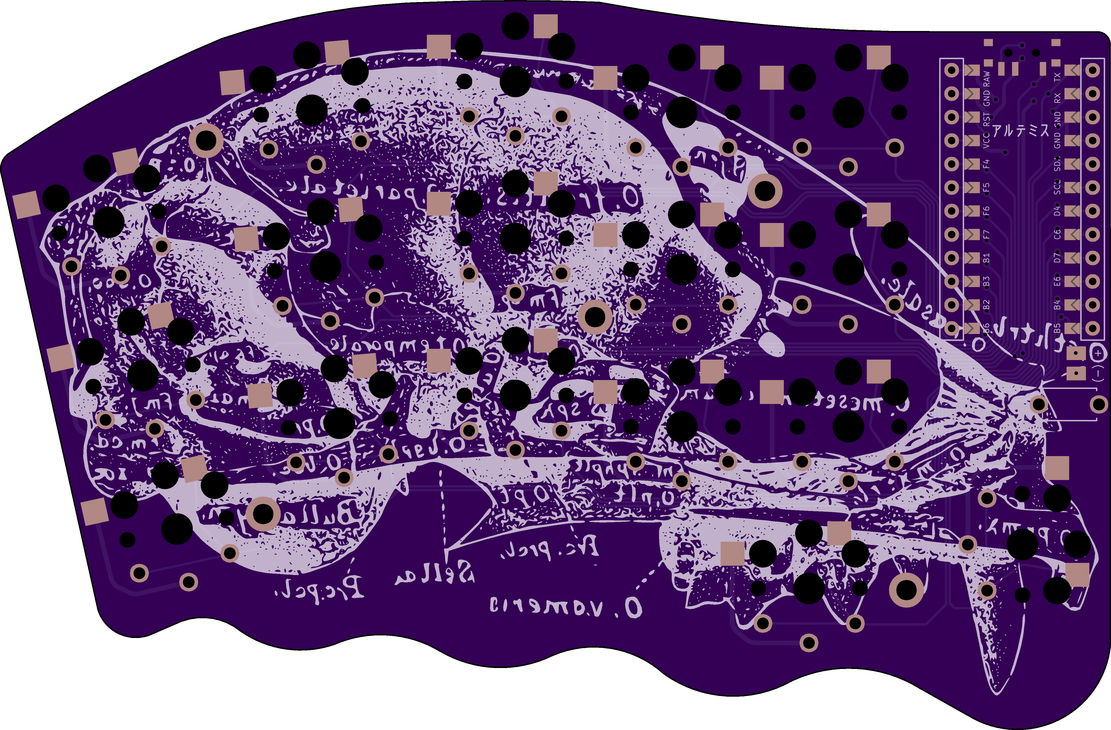
2 layers119.9 × 77.8 mmArtemis, the printed circuit board in 3D

bluetooth-only low-profile choc-spaced smol split keyboards

Size
119.9 × 77.8 mm
Copper layers
2
Thickness
1.6 mm
Parts
28
Nets
24
Pads
428
Tracks, vias
1,040, 31
Routed
Yes
KiCad
KiCad 6 (file 20211014)
Created
6 Jan 2022
Updated
25 Jan 2022

Overview

Artemis is an open-source printed circuit board by mindhatch, from the mindhatch/keyboards repository on GitHub, published under the MIT licence. It is a 2-layer board of 119.9 × 77.8 mm with 28 parts on 24 nets, routed with 1,040 tracks and 31 vias.

Its parts include 18 switches and 1 IC. It belongs with the keyboards and input boards and the AVR (ATmega, ATtiny) boards of this library.

README

README.md

keyboards!

  • 30-34 keys
  • choc-spaced
  • bluetooth-only
  • 1.5u thumb keys
  • column staggered
  • splayed ring and pinky columns
  • mcu footprint fits spring-loaded pin headers

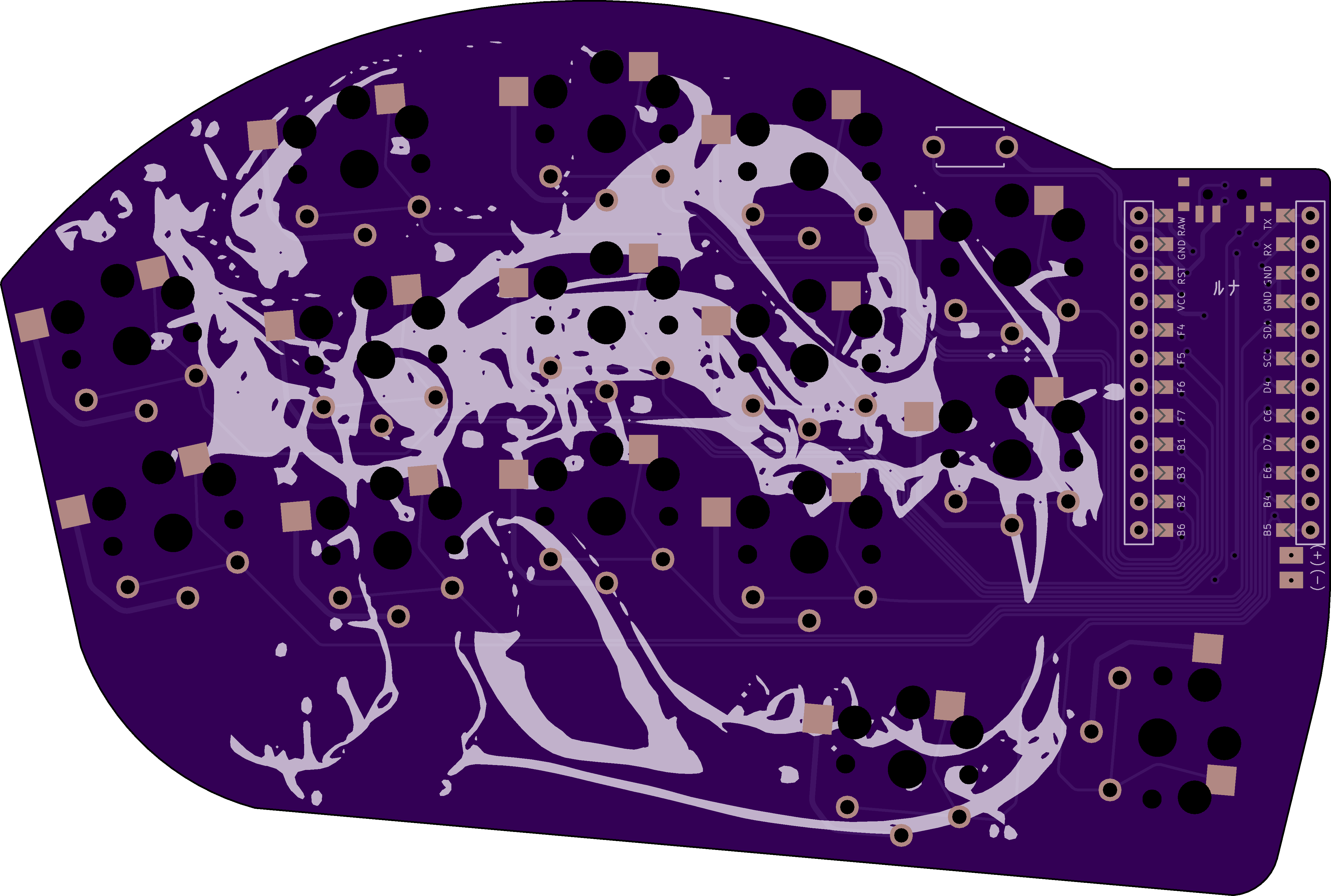
ルナ (luna)

  • 30 keys
  • 5° splay on ring column
  • 12.5° splay on pinky column
  • switches can be soldered or used with hotswap sockets
  • firmware can be found here


luna_left

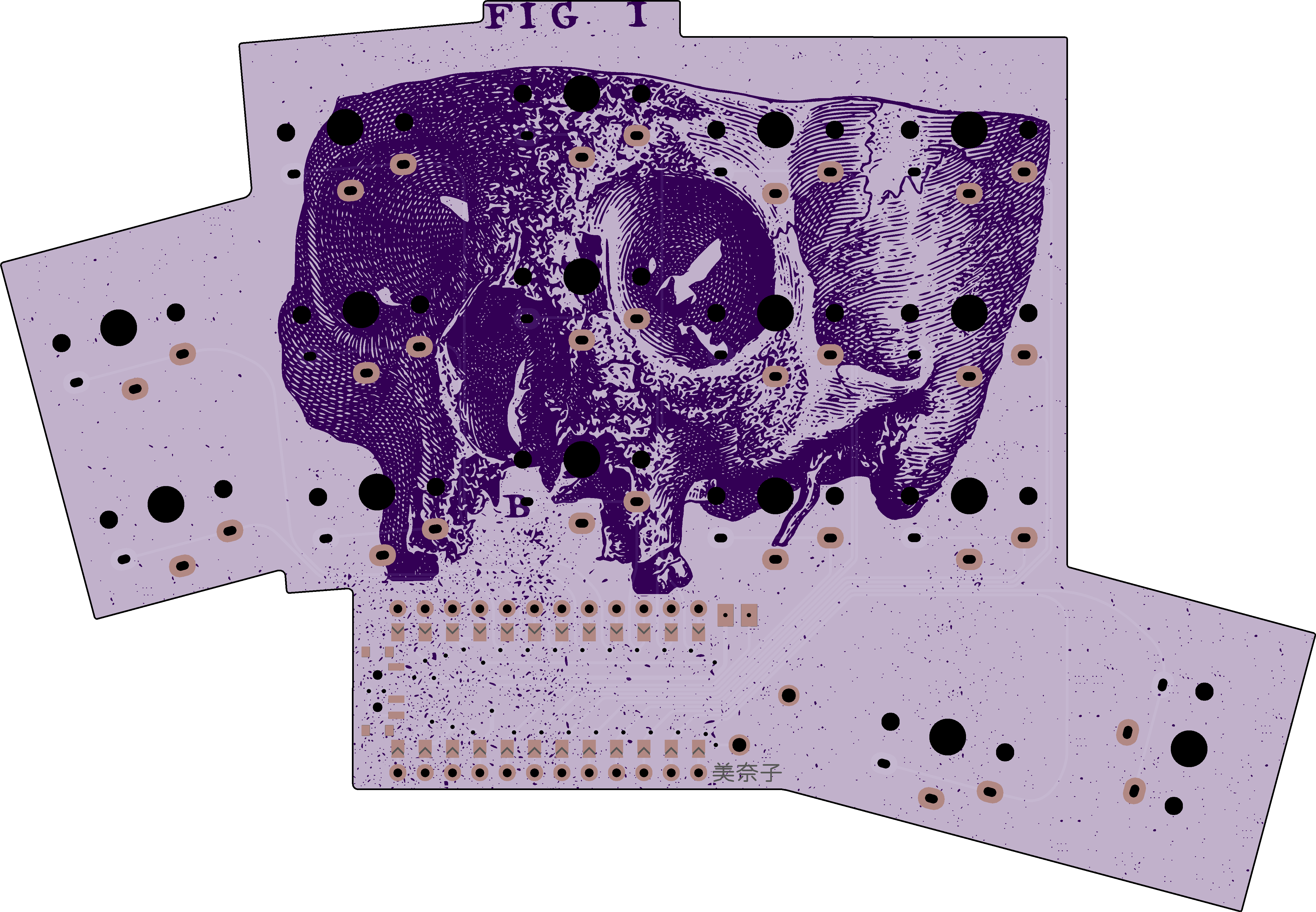
美奈子 (minako)

  • 32 keys
  • 5° splay on ring column
  • 15° splay on pinky column
  • switches are solder-only
  • firmware can be found here


minako_left

アルテミス (artemis)

  • 34 keys
  • 5° splay on ring column
  • 12.5° splay on pinky column
  • switches can be soldered or used with hotswap sockets
  • firmware can be found here


artemis_left

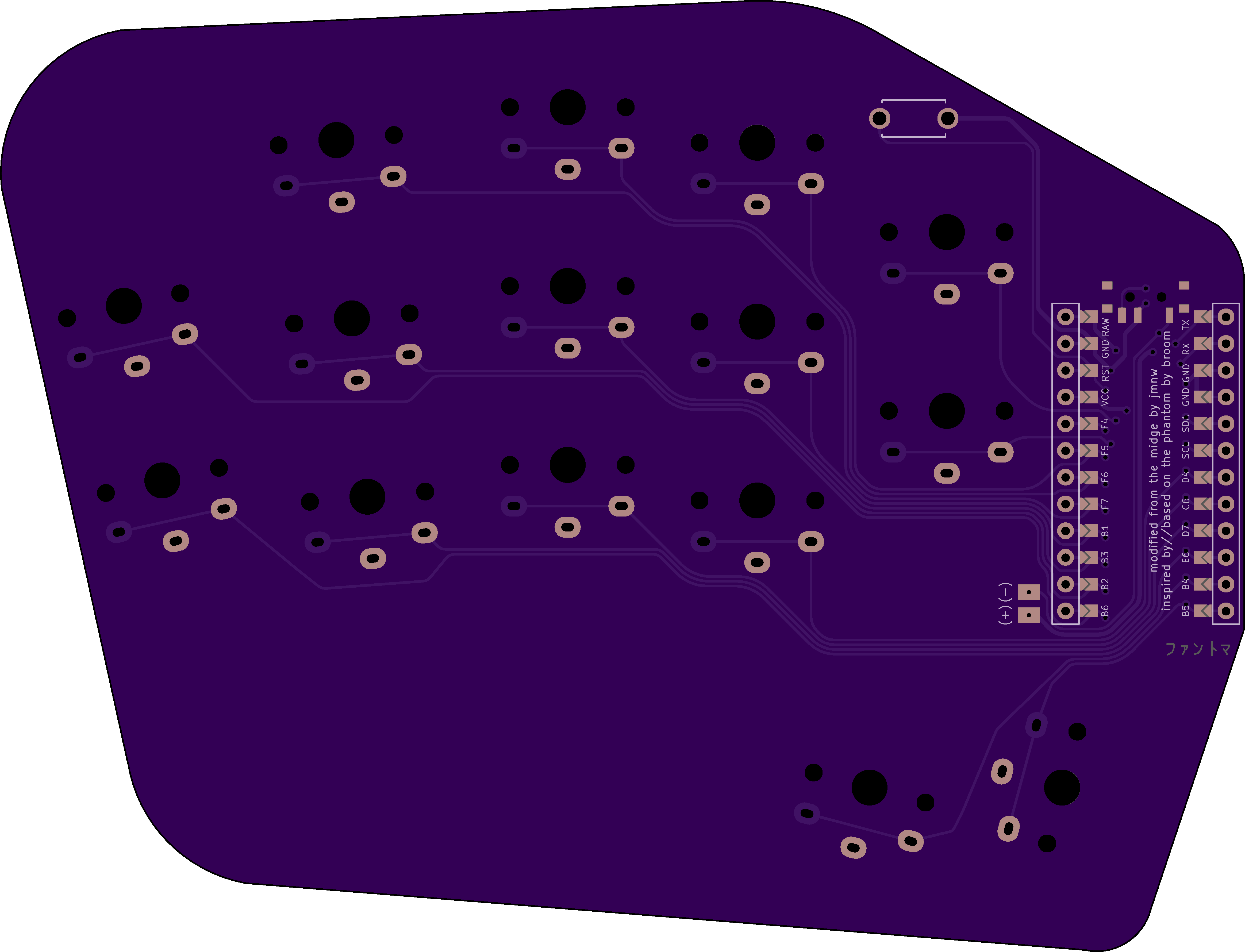
ファントマ (la phantoma)

  • 30 keys
  • 5° splay on ring column
  • 12.5° splay on pinky column
  • switches are solder-only
  • directly inspired by and based on le phantom by broom
  • firmware can be found here


phantoma_left


microcontroller footprint designed by Jimmerricks based on a design by 50an6xy06r6n
waterfall traces inspired by enzocoralc

Parts

28
QtyValueFootprintReferences
15Kailh_socket_PG1350_optional_reversiblebugs:Kailh_socket_PG1350_optional_reversible_1uSW1, SW2, SW3, SW4, SW5, SW6, SW7, SW8, SW9, SW10, SW11, SW12, SW13, SW14, SW15
2Kailh_socket_PG1350_optional_reversiblebugs:Kailh_socket_PG1350_optional_reversible_15uSW16, SW17
2LOGOLOGOCATSKULLB, CATSKULLF
1Battery_Cellbugs:Battery_pads_reversibleBT1
1ProMicrobugs:ProMicro_jumpersU1
1SW_Pushkbd:ResetSWSW18
1SW_SPDTbugs:Power_reversiblePSW1

The 23 most common of 28 parts.

Questions

How big is the Artemis PCB?

It measures 119.9 × 77.8 mm and has 2 copper layers, 1.6 mm thick.

What parts does the Artemis use?

28 parts. The full list of its parts is on this page, with links to each part's symbol and footprint where PCBKit's library has them.

Where can I download the Artemis KiCad files?

From the mindhatch/keyboards repository on GitHub, at the commit this page was made from: the board is pcbs/artemis/artemis.kicad_pcb and its schematic pcbs/artemis/artemis.kicad_sch. PCBKit opens the board in the browser, with nothing to install.

Can I use the Artemis design in my own project?

Its repository publishes it under the MIT licence: you may reuse it on that licence's terms (keep the author's notice, and for a copyleft licence share your changes alike).

More from mindhatch/keyboards

3
  • 2 layers122.1 × 84.6 mmMinako, the printed circuit board in 3D

    Minako

    mindhatch/keyboards

    bluetooth-only low-profile choc-spaced smol split keyboards

    22 parts57MIT
  • 2 layers118.1 × 77.8 mmLuna, the printed circuit board in 3D

    Luna

    mindhatch/keyboards

    bluetooth-only low-profile choc-spaced smol split keyboards

    21 parts57MIT
  • 2 layers118 × 90.2 mmPhantoma, the printed circuit board in 3D

    Phantoma

    mindhatch/keyboards

    bluetooth-only low-profile choc-spaced smol split keyboards

    19 parts57MIT

Similar boards

  • 2 layers44.5 × 72.7 mmOSO SWAT C1-jig, the printed circuit board in 3D

    OSO SWAT C1-jig

    joeycastillo/Sensor-Watch

    A board replacement for the classic Casio F-91W wristwatch

    28 parts2.1k
  • 2 layers95 × 54 mmEinkPDA screen, the printed circuit board in 3D

    EinkPDA screen

    TalismanDesign/PocketMage_PDA

    An E-Ink PDA device using the ESP32 S3.

    28 parts2kApache-2.0
  • 2 layers45 × 45 mmSmartbuttons, the printed circuit board in 3D

    Smartbuttons

    hackclub/OnBoard

    💡 Join 1,000 teenagers and make your first PCB with a $100 grant!

    28 parts915
  • 2 layers24.1 × 36.2 mmEsp32miniBT, the printed circuit board in 3D

    Esp32miniBT

    asterics/esp32_mouse_keyboard

    ESP32 implementation for HID over GATT Keyboard and Mouse (Bluetooth Low Energy). Including serial API for external modules (similar to Adafruit EZKey HID)

    28 parts911GPL-3.0
  • 2 layers34.8 × 12.2 mmInfnoise goldfingers, the printed circuit board in 3D

    Infnoise goldfingers

    waywardgeek/infnoise

    The world's easiest TRNG to get right

    28 parts854CC0-1.0
  • 2 layers55.9 × 99.1 mmStm32f0 disco Luos shield, the printed circuit board in 3D

    Stm32f0 disco Luos shield

    Luos-io/luos_engine

    Open-source and real-time orchestrator for cyber-physical-systems, to easily design, test and deploy embedded applications and digital twins.

    28 parts546MIT
  • 2 layers88 × 25 mmEleLab v2 Frontpanel a, the printed circuit board in 3D

    EleLab v2 Frontpanel a

    Chrismettal/EleLab_v2

    Cheap DIY lab system for hobbyists and the tinkering folk

    28 parts531GPL-3.0