4 layers62.1 × 83.8 mm
Ss main board
loopj/short-stack
World's Smallest Nintendo Wii, using a trimmed motherboard and custom stacked PCBs
69 parts804

 mattvenn/vga_clock_pcb30
Open source hardware down to the chip level!
Carrier is an open-source printed circuit board by mattvenn, from the mattvenn/vga_clock_pcb repository on GitHub, published under the MIT licence. It is a 2-layer board of 30 × 48 mm with 40 parts on 67 nets, routed with 433 tracks and 49 vias.
It is built around the MIC5504-3.3YM5-TR and ECS-5032MV-100-BN-TR. Its parts include 8 capacitors, 7 resistors, 3 ICs, 3 connectors and 3 switches.


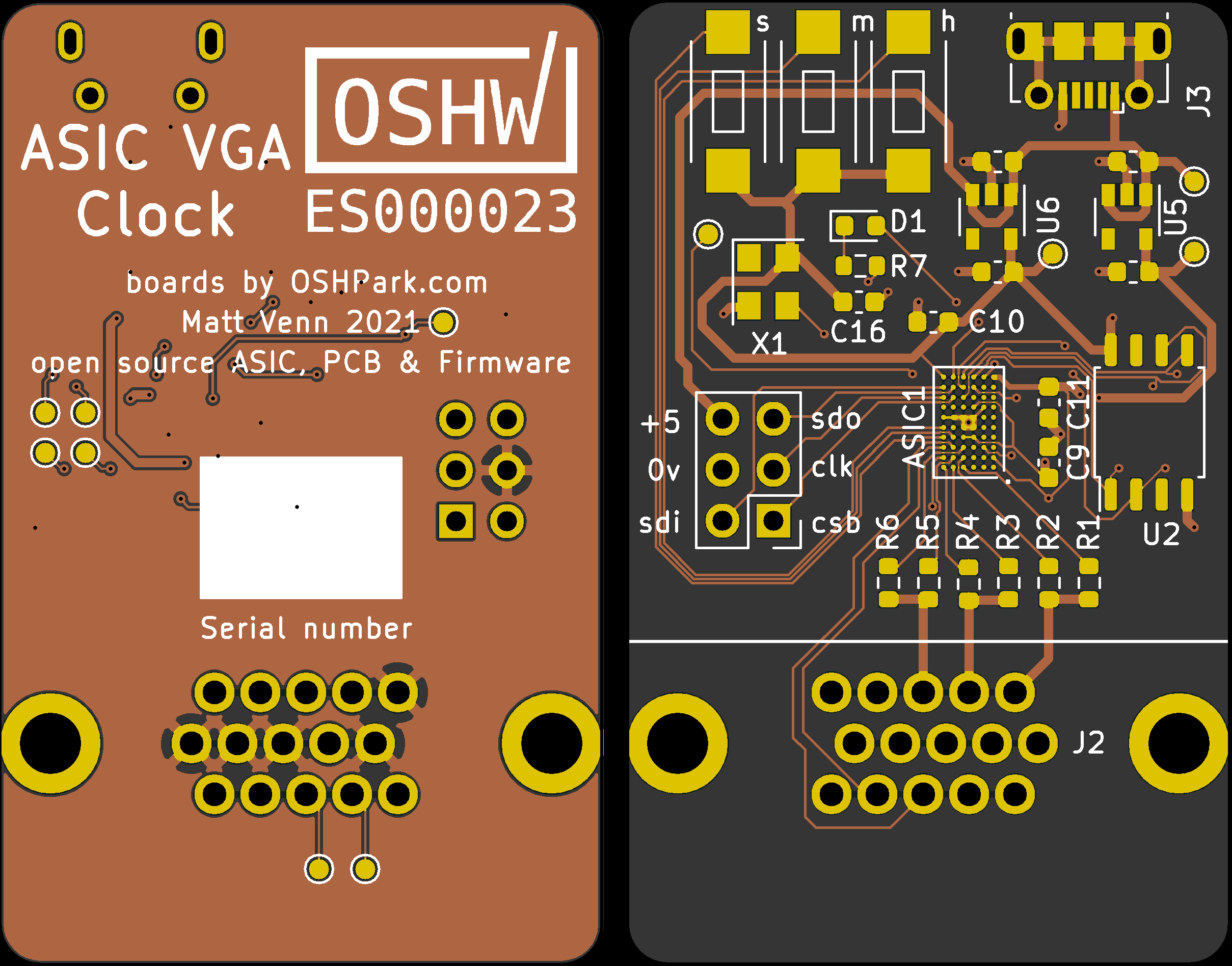
This PCB provides all the necessary components to make a functional clock:
Needs to active project 2. See https://github.com/mattvenn/caravel-mph/blob/release/verilog/dv/caravel/user_proj_example/vga-clock/vga_clock.c for the simulation test. Will need PLL setup to work on the ASIC.
For flashing, see https://github.com/efabless/ravenna/blob/master/firmware/blink/Makefile as a starting point. ravenna_hkspi.py may need some tweaks to work with Caravel.
The SPI interface can be used to put the ASIC into 'passthrough' mode. Then the FLASH can be programmed through this same SPI interface.
See the schematic for the pinout of the SPI interface on the board.
Needs 31.5MHz for VGA signal. As precise as possible for good timekeeping. Input oscillator is 9MHz.
Using https://github.com/kbeckmann/caravel-pll-calculator
matt-desktop:2003 [main]: ./caravel_pll.py generate --clkout 31.5 --clkin 9
PLL Parameters:

clkin:    9.00 MHz
clkout:   31.50 MHz
clkout90: 31.50 MHz

PLL Feedback Divider: 14
PLL Output Divider 1: 4
PLL Output Divider 2: 4

Register 0x11: 0x24
Register 0x12: 0x0eSee the instantiation into the user project area here: https://github.com/mattvenn/multi-project-harness/blob/separate-macro/user_project_wrapper.v#L190 See the design repository here: https://github.com/mattvenn/vga-clock/tree/db029c38607c8d27f54b48bd8fd423cae3c4ed3d
vga_clock proj_2 (
    .clk(proj2_clk),
    .reset_n(proj2_reset),
    .adj_hrs(proj2_io_in[8]),
    .adj_min(proj2_io_in[9]),
    .adj_sec(proj2_io_in[10]),
    .hsync(proj2_io_out[11]),
    .vsync(proj2_io_out[12]),
    .rrggbb(proj2_io_out[18:13])
);All available from digikey as of 13/7/21
This board is an OSHWA approved design: ES000023
| Qty | Value | Footprint | References |
|---|---|---|---|
| 12 | TestPoint | TestPoint:TestPoint_Pad_D1.0mm | TP1, TP2, TP3, TP4, TP5, TP6, TP7, TP8, TP9, TP10, TP11, TP12 |
| 4 | 22n | Capacitor_SMD:C_0603_1608Metric | C9, C10, C11, C16 |
| 3 | 1k | Resistor_SMD:R_0603_1608Metric | R2, R4, R6 |
| 3 | 500R | Resistor_SMD:R_0603_1608Metric | R1, R3, R5 |
| 2 | 1u 16v | Capacitor_SMD:C_0603_1608Metric | C1, C5 |
| 2 | 4u7 16v | Capacitor_SMD:C_0603_1608Metric | C3, C7 |
| 1 | 100R | Resistor_SMD:R_0603_1608Metric | R7 |
| 1 | CARAVEL | carrier:WLCSP-60_P0.5mm | ASIC1 |
| 1 | Conn_02x03_Counter_Clockwise | Connector_PinHeader_2.54mm:PinHeader_2x03_P2.54mm_Vertical | J1 |
| 1 | DB15_Female_HighDensity | carrier:db15 | J2 |
| 1 | ECS-5032MV-100-BN-TR | Oscillator:Oscillator_SMD_SeikoEpson_SG8002CE-4Pin_3.2x2.5mm | X1 |
| 1 | LED | LED_SMD:LED_0603_1608Metric | D1 |
| 1 | LOGO | carrier:oshw-logo-small | G*** |
| 1 | MCP1824T-1802E/OT | Package_TO_SOT_SMD:SOT-23-5 | U5 |
| 1 | MIC5504-3.3YM5-TR | Package_TO_SOT_SMD:SOT-23-5 | U6 |
| 1 | SW_Push_hrs | carrier:pts636 | SW1 |
| 1 | SW_Push_min | carrier:pts636 | SW2 |
| 1 | SW_Push_sec | carrier:pts636 | SW3 |
| 1 | USB_B_Micro | Connector_USB:USB_Micro-B_Molex-105017-0001 | J3 |
| 1 | W25Q32JVSSIQ-TR | Package_SO:SOIC-8_5.23x5.23mm_P1.27mm | U2 |
loopj/short-stack
World's Smallest Nintendo Wii, using a trimmed motherboard and custom stacked PCBs

MicroCoreLabs/Projects
Ted Fried's MicroCore Labs Projects - FPGA CPU cores and emulators for the 8088, 8086, 8051, 6502, 68000, Z80, Risc-V, and also Typewriter and EPROM Emulator projects.

tinyfpga/TinyFPGA-B-Series
Open source design files for the TinyFPGA B-Series boards.


alvarop/swd2usbc
Have you ever wanted to debug your device over USB-C? Sometimes there's not enough room for a JTAG/SWD connector, or even Tag-Connect pads!

PetteriAimonen/esp-walkie-talkie-hw
Hardware for ESP8266 based walkie talkie (doesn't work particularly well)

It measures 30 × 48 mm and has 2 copper layers, 1.6 mm thick.
40 parts, built around the MIC5504-3.3YM5-TR and ECS-5032MV-100-BN-TR. The full list of its parts is on this page, with links to each part's symbol and footprint where PCBKit's library has them.
From the mattvenn/vga_clock_pcb repository on GitHub, at the commit this page was made from: the board is carrier.kicad_pcb. PCBKit opens the board in the browser, with nothing to install.
Its repository publishes it under the MIT licence: you may reuse it on that licence's terms (keep the author's notice, and for a copyleft licence share your changes alike).