4 layers33.7 × 12.4 mm
Display eval short
byrantech/laptop
anyon_e, a highly integrated, high end, open source laptop. Attempt the impossible.
4 parts4.3kMIT
 markomij12/PDN-CoSimulation
KiCad → openEMS validator → SPICE / plane PDN optimizer (decap BOM + |Z(f)|)
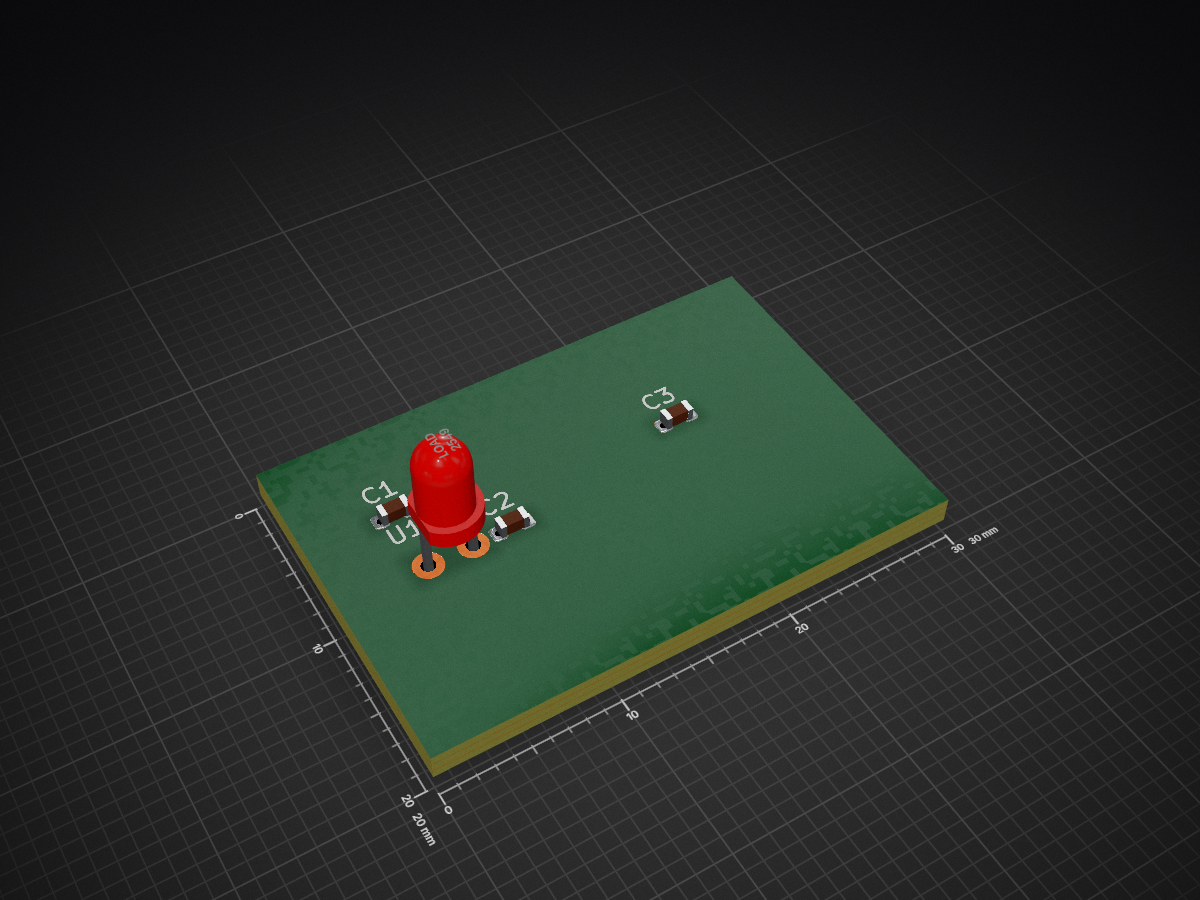
Pdn test is an open-source printed circuit board by markomij12, from the markomij12/PDN-CoSimulation repository on GitHub, published under the MIT licence. It is a 4-layer board of 30 × 20 mm with 4 parts on 2 nets.
Its parts include 3 capacitors and 1 IC.
Phase 1 is still the analytical plate in em_extraction.geometry, not a layout file.
Phase 2 board: pdn_test.kicad_pcb — a small 4-layer FR-4 coupon for the KiCad → openEMS bridge. You don't need the KiCad GUI; read_board() parses the s-expression in the project venv.
pdn_test.kicad_pcb| Item | Value |
|---|---|
| Size | 30 mm × 20 mm (Edge.Cuts rectangle at the origin) |
| Stackup | 1.6 mm FR-4-ish, 35 µm copper |
| F.Cu / B.Cu | signal (unused by the extractor) |
| In1.Cu | VCC power plane |
| In2.Cu | GND plane |
| Inner dielectric | 0.2 mm prepreg, εr = 4.5 (the PDN cavity, In1.Cu ↔ In2.Cu) |
| Core | 1.04 mm, εr = 4.5, F.Cu↔In1.Cu |
| Bottom prepreg | 0.2 mm, εr = 4.5, In2.Cu↔B.Cu |
The .kicad_pcb text file stores millimetres (KiCad's internal unit is nm). em_extraction.kicad_reader.read_board converts millimetres → metres in BoardGeometry.
read_board() identifies ports by names, not hardcoded xy:
| Role | How it is identified |
|---|---|
| Power net | VCC |
| Ground net | GND |
| IC power pin | footprint reference U1, pad on net VCC |
| Candidate decap sites | vias on net VCC |
U1 is a dummy 2-pin load (pad 1 = VCC, pad 2 = GND). C1 and C2 sit next to U1; C3 is farther out so the optimizer has a near/far placement choice. Move a VCC via in KiCad and re-run python run_pipeline.py --board boards/pdn_test.kicad_pcb to change the extracted S-parameters.
To add another decap candidate, place a via on net VCC. To move the IC pin, move footprint U1.
| Qty | Value | Footprint | References |
|---|---|---|---|
| 3 | C | Capacitor_SMD:C_0603_1608Metric | C1, C2, C3 |
| 1 | LOAD | PDN:Load_2pin | U1 |
byrantech/laptop
anyon_e, a highly integrated, high end, open source laptop. Attempt the impossible.

dotstartech/wall-panel
Wall mounted 4 inch touch display panel with CM4 inside


Hongcheng-Gao/EngiWorld
Engiworld: What Can Frontier Agents Deliver in Professional Engineering Environments?

OpenDevicePartnership/pico-de-gallo
A tool for testing Embedded Rust drivers for discrete I2C/SPI components.

azonenberg/misc-devboards
Miscellaneous prototype hardware that wasn't major enough to warrant a dedicated repo

It measures 30 × 20 mm and has 4 copper layers, 1.6 mm thick.
4 parts. The full list of its parts is on this page, with links to each part's symbol and footprint where PCBKit's library has them.
From the markomij12/PDN-CoSimulation repository on GitHub, at the commit this page was made from: the board is boards/pdn_test.kicad_pcb. PCBKit opens the board in the browser, with nothing to install.
Its repository publishes it under the MIT licence: you may reuse it on that licence's terms (keep the author's notice, and for a copyleft licence share your changes alike).