2 layers52.2 × 52.2 mm
Base
google/mozc-devices
Circuit diagrams and firmware source code for Gboard DIY keyboards
43 parts3kApache-2.0

 MarkDunne/balance-bot
Two-wheel self-balancing robot motherboard PCB — schematic in SKiDL, placement in pcbnew
Balance bot is an open-source printed circuit board by MarkDunne, from the MarkDunne/balance-bot repository on GitHub. It is a 2-layer board of 100 × 80 mm with 43 parts on 39 nets, routed with 395 tracks and 107 vias.
Its parts include 12 resistors, 11 connectors, 7 capacitors, 3 diodes and 3 transistors. It belongs with the robots and motor control and computers and single-board computers boards of this library.
A two-wheel self-balancing robot. This repo currently holds the hardware design: a passive motherboard PCB that every module plugs into.
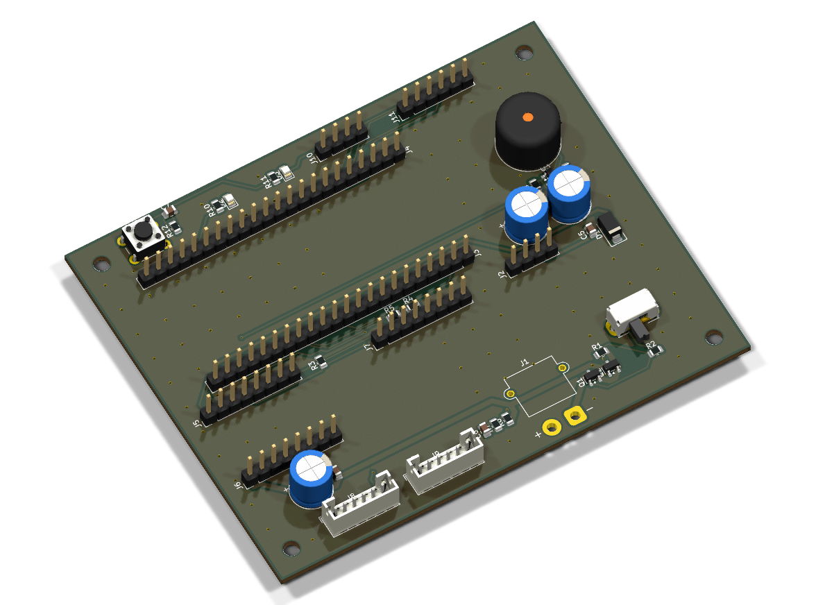
100 × 80mm, 2-layer, routed and poured, DRC-clean. Every image here is
generated by just render from the board file — nothing is drawn by hand,
including the routing.
The schematic is Python. hardware/balance_bot.py is the single source of
truth for the netlist and the pin map — nothing is transcribed by hand
between them, so they cannot drift apart.
just bootstrap    # clone KiCad symbol libraries, sync the venv
just check        # build the netlist, run the design rules
just check writes build/balance_bot.net and regenerates docs/pinmap.md.
KiCad is not needed for any of that — only for laying out the board.
The netlist is committed on purpose. It is deterministic, so git diff on it
shows exactly what a change to the schematic did to the connectivity.
just view # -> build/board.htmlEvery socket rendered pin by pin, with click-to-trace net highlighting — the view you want when wiring the thing up or checking a module pinout. Generated from the circuit, so it cannot go stale.
just svg # -> build/schematic.svg (needs: pnpm add -g netlistsvg)A schematic-style drawing with proper symbols, refdes and values. Good for
spotting a wrong part; not a schematic you would hand to someone, because
SKiDL feeds netlistsvg pin numbers rather than pin names and emits no net
labels. See hardware/schematic_svg.py for why patching that around makes it
worse.
SKiDL's generate_schematic hangs on this circuit — don't bother. For a real
board, use KiCad.
just checkjust route — places, routes, pours ground and runs DRC, no GUI involvedRe-running just check after a schematic change and re-importing updates the
board without disturbing what is already placed — refdes are pinned in the
source rather than auto-numbered.
docs/workflow.md — how this board was designed, the
tooling gotchas, what the checks catch and what they miss, and how to start
the next onedocs/design.md — architecture, power budget, the
decisions worth knowing about, and what to verify before ordering boardsdocs/mechanical.md — board envelope and mounting, for
designing the chassisdocs/fab.md — PCBWay order parameters and what gets uploadeddocs/pinmap.md — generated pin assignmentsdocs/bom.md — shopping listjust board # generate hardware/balance_bot.kicad_pcb from the netlist
just netclasses # trace widths, derived from the currents in docs/design.md
just route # board -> DSN -> Freerouting -> SES -> board -> pour -> DRC
just pour # ground plane on both layers, stitched (part of `just route`)
just plot # look at the placement
just drc # headless design rule check
just fab # DRC, then Gerbers + drill -> build/balance-bot-fab.zipjust board places every footprint, draws the outline and mounting holes, and
assigns all 38 nets. just route then calls it, autoroutes, pours ground and
runs DRC — so the board is regenerated from source each time rather than
edited in place, and re-running gives the same board.
That holds only while every track came out of the autorouter. The moment you
hand-route anything in Pcbnew, just board and just route both destroy it,
and from that point the .kicad_pcb is the artifact — schematic changes go in
through Pcbnew's netlist re-import instead.
Placement is checked in the script rather than by eye: every courtyard is tested against every other and against the mounting-hole keepouts, and the build fails on a clash. That includes the modules that plug in on top: a socket's courtyard is its pin row, while the module is a PCB many times the size, so the check uses the module outline instead. Flat SMD may sit underneath; through-hole parts may not.
just fab runs DRC first and refuses to produce an upload package if it
fails — so an unrouted or violating board cannot reach PCBWay.
Schematic complete and checked. Board placed, clear, routed and poured:
all 99 connections routed, ground on both layers stitched into one plane, and
DRC reports 0 violations and 0 unconnected items. just fab produces an
upload package. No firmware yet.
Routing is generated, not drawn — just route runs the whole chain and is
reproducible, so the board can be regenerated from source rather than
preserved. That is the opposite of the usual advice and the reason the
warning about never re-running just board is now narrower than it was: it
holds only once something is hand-routed.
| Top | Bottom |
|---|---|
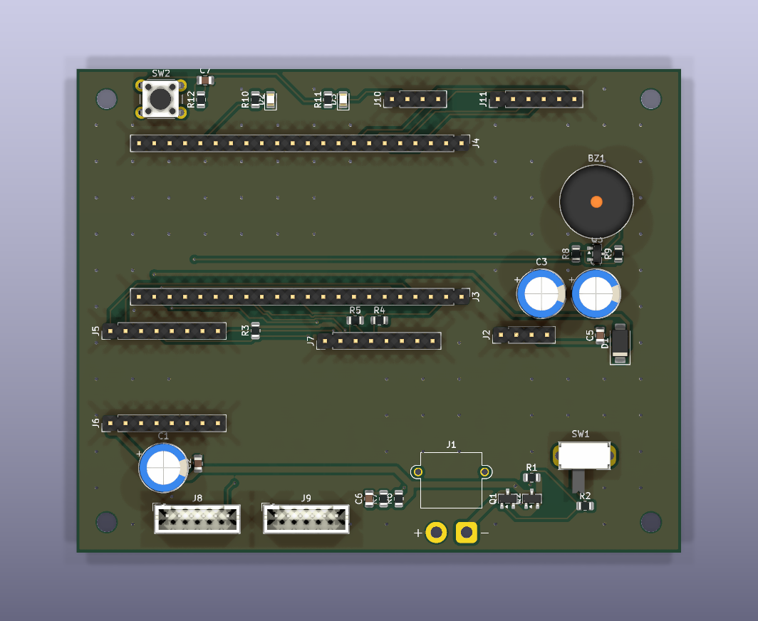 | 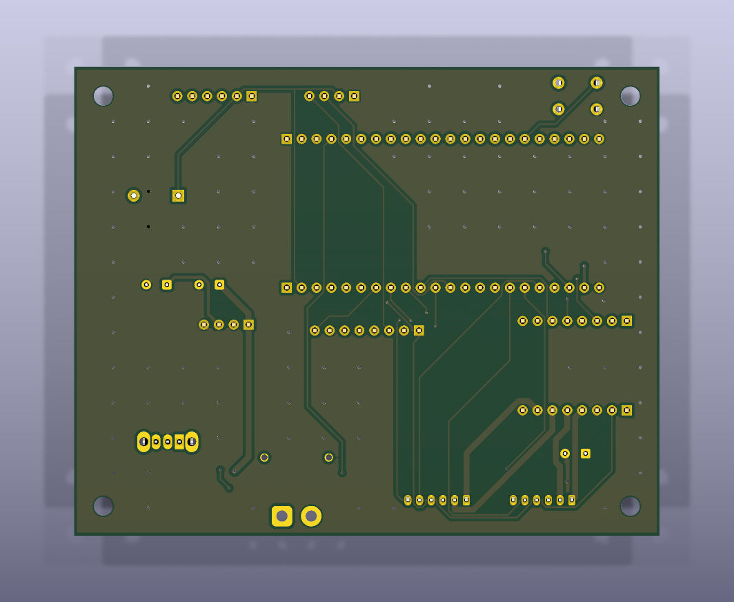 |
The bottom is the clearer look at the routing: gold pads, traces, and the regular grid of stitching vias tying the two ground planes together. Most of what looks like bare board on both sides is ground pour.
The placement was solved against the checks rather than drawn: the floorplan
is a design decision — USB left, motors and battery bottom, switch right, IMU
centred laterally — and each passive then sits as close to what it serves as
the module outlines allow. The module outlines are still assumed, not
measured, and the whole layout rests on them. See the checklist in
docs/design.md before ordering.
100 × 80mm, 2-layer, hand-soldered; motors mount to the chassis rather than the
board. See docs/mechanical.md to design the chassis in parallel.
| Qty | Value | Footprint | References |
|---|---|---|---|
| 12 | R_0805_2012Metric | R_0805_2012Metric | R1, R2, R3, R4, R5, R6, R7, R8, R9, R10, R11, R12 |
| 4 | C_0805_2012Metric | C_0805_2012Metric | C2, C5, C6, C7 |
| 4 | MountingHole_3.2mm_M3 | MountingHole_3.2mm_M3 | H1, H2, H3, H4 |
| 3 | CP_Radial_D8.0mm_P3.50mm | CP_Radial_D8.0mm_P3.50mm | C1, C3, C4 |
| 3 | PinHeader_1x08_P2.54mm_Vertical | PinHeader_1x08_P2.54mm_Vertical | J5, J6, J7 |
| 3 | SOT-23 | SOT-23 | Q1, Q2, Q3 |
| 2 | JST_PH_B6B-PH-K_1x06_P2.00mm_Vertical | JST_PH_B6B-PH-K_1x06_P2.00mm_Vertical | J8, J9 |
| 2 | LED_0805_2012Metric | LED_0805_2012Metric | D2, D3 |
| 2 | PinHeader_1x04_P2.54mm_Vertical | PinHeader_1x04_P2.54mm_Vertical | J2, J10 |
| 2 | PinHeader_1x22_P2.54mm_Vertical | PinHeader_1x22_P2.54mm_Vertical | J3, J4 |
| 1 | AMASS_XT30PW-M_1x02_P2.50mm_Horizontal | AMASS_XT30PW-M_1x02_P2.50mm_Horizontal | J1 |
| 1 | Buzzer_12x9.5RM7.6 | Buzzer_12x9.5RM7.6 | BZ1 |
| 1 | D_SMA | D_SMA | D1 |
| 1 | PinHeader_1x06_P2.54mm_Vertical | PinHeader_1x06_P2.54mm_Vertical | J11 |
| 1 | SW_PUSH_6mm_H5mm | SW_PUSH_6mm_H5mm | SW2 |
| 1 | SW_Slide_SPDT_Angled_CK_OS102011MA1Q | SW_Slide_SPDT_Angled_CK_OS102011MA1Q | SW1 |
google/mozc-devices
Circuit diagrams and firmware source code for Gboard DIY keyboards

rusefi/rusefi
rusefi - GPL internal combustion engine control unit


jrsteensen/OpenHornet
OpenHornet 1:1 F/A-18C Simulator Repository


tebl/RC6502-Apple-1-Replica
An expandable SBC-version of the Apple 1 computer, easy to get started with and lot of cool stuff that can be added to it!

nodestark/mdb-esp32-cashless
ESP32-based MDB cashless device for vending machines, supporting EVA DTS DEX/DDCMP telemetry and payments over the MDB protocol via Bluetooth and MQTT

zynthian/zynthian-hw
Zynthian hardware stuff: PCBs, schemes, parts specifications, pin assignment, ...
It measures 100 × 80 mm and has 2 copper layers, 1.6 mm thick.
43 parts. The full list of its parts is on this page, with links to each part's symbol and footprint where PCBKit's library has them.
From the MarkDunne/balance-bot repository on GitHub, at the commit this page was made from: the board is hardware/balance_bot.kicad_pcb. PCBKit opens the board in the browser, with nothing to install.
Its repository states no licence, so its author keeps all rights: ask MarkDunne before reusing the design.