2 layers188 × 102.9 mm
RC200-Dev Backplane
MarkD833/RCBUS-68xxx
My Motorola 68000 & 68302 processors (+ SIO, PIO & MFP boards) for the RCBus ecosystem.
102 parts8GPL-3.0

 MarkD833/RetroDuino-8085
8085 Microprocessor system on an Arduino UNO'ish footprint
0025 8085 UNO Board W65C22 v2 is an open-source printed circuit board by MarkD833, from the MarkD833/RetroDuino-8085 repository on GitHub, published under the GPL-3.0 licence. It is a 4-layer board of 76.2 × 53.3 mm with 42 parts on 100 nets, routed with 1,309 tracks and 64 vias.
It is built around the 74LS573PC, AMS1117-3.3 and DS1233-10+T&R, with the W27C512-45Z among its other parts. Its parts include 16 capacitors, 10 ICs, 7 resistors, 3 connectors and 2 diodes. It belongs with the AVR (ATmega, ATtiny) and FPGA and CPLD boards of this library.


I've been toying with the idea of creating an 8085 based microprocessor board around the size of an Arduino UNO ever since I came across the 65uino board on the hackaday website.
I started off with some basics:
| Item | Notes |
|---|---|
| Microprocessor | an 8085 device but which one and what clock speed |
| ROM | At least 8K maybe 16K - but do I need that much? |
| RAM | 32K would be good to aim for |
| Serial | 1 serial port but bit bang or hardware? |
| I/O | Bit programmable i/o |
| Analogue In | A multi channel ADC if there's room |
| LEDs | At least 1 user LED |
Oh, and one other requirement - no surface mount chips or hard to solder parts!
That's quite a lot to cram into the footprint on an Arduino UNO!
After a lot of playing around with an Arduino UNO prototyping board and various chip sockets I came up with a basic design and layout.
The 8085 is mostly seen in a 40-pin DIL package. That's a huge amount of real estate on a footprint the size of an Arduino UNO. I discovered that OKI Semiconductor manufactured an 80C85 in a 44-pin PLCC package (MSM80C85AHGS-2K). After a quick bit of digging I located the datasheet and also a source on ebay that was selling some of the chips as NOS (New Old Stock).
Additional board space is consumed as the 8085 has a multiplexed address and data bus. The lower 8-bits are shared between D0..D7 and A0..A7 and an 8-bit latch (74LS573) is used to capture A0..A7.
Another design challenge is that the 8085 interrupts (if I were to use them) are active high rather than active low!
The 8085 is clocked from an 11.0592MHz crystal, which gives an actual clock of 5.5296MHz (the 8085 divides the crystal frequency by 2). I've yet to experiment to see the effects of a higher frequency even though I'm exceeding the manufacturers 10MHz clock by 10% already.
There are quite a few ROM devices available in a PLCC package as well, but I decided to go with a Winbond W27C512 64K x 8 EEPROM in a 28-pin DIL package. There's plenty for sale on ebay too. The reason for going the DIL package route will become clear with the choice of RAM device.
I couldn't find any suitable RAM devices in PLCC format so the project success was looking rather bleak. Then I discovered that there were some SRAM devices available in DIL packages that were only 0.3in wide (called Skinny-DIP if I recall correctly). I then got lucky and sourced some UMC UM61512AK 64K x 8 SRAMs in a skinny 32-pin DIL package.
The RAM chip could sit underneath the ROM chip and I would save a lot of board space.
I thought about bit banging the serial port using the SID and SOD pins of the 8085 but decided to try and go with real hardware. Again board space was at a premium so the hunt was on for a small UART device. A lot of serial chips have a large number of pins dedicated to various handshaking signals as well as synchronous data transfer - although some devices allow repurposing of these signals as discrete inputs or outputs. They are all still quite large chips in either PLCC or 0.6in DIL packages.
I then discovered a Philips SCC2691 UART (SCC2691AC1N24) that was available in a 0.3in wide 24-pin DIL package. It had an internal baud rate generator and a single 16-bit timer/counter as well.
I really wanted the I/O chip to have pin programmable direction control. That ruled out the 8155 and 8255 chips. It took a lot of searching but I then discovered a Zilog Z85C36. It had 2x 8-bit bit programmable I/O ports as well as 3x 16-bit timer/counters. That would be perfect!
Except that it wasn't! In my v1.0 design, I couldn't get the Z85C36 to respond at all. I don't know quite what the issue was as I was sure that I was meeting the timing requirements - but clearly something wasn't right.
In order to salvage the situation, I changed the I/O chip to a WDC W65C22S device. The chip still gave me 2x 8-bit bit programmable I/O ports, but only 2x 16-bit timer/counters.
If I could fit it in, then an a National Semiconductor ADC0844 might work out - it's a 4 channel ADC in a 20-pin DIL package.
There was quite a bit of massaging to get everything to fit as I also used a GAL16V8 to handle address decoding and interrupt inversion. The result was a board slightly longer than an Arduino UNO (but the same width).
This is an annotated 3D view of the board generated by Kicad as it stands at v1.2.
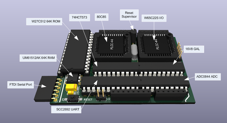
The thick white lines on the silkscreen just to the right of the FTDI serial port connector and the ADC0844 chip show the outline of an actual Arduino UNO board.
Assembly of the board is pretty straightforward with a few things of note.
This is a photo of the RetroDuino-8085 board showing the location of the 3.6864MHz UART crystal and the modified 28-pin DIL socket.
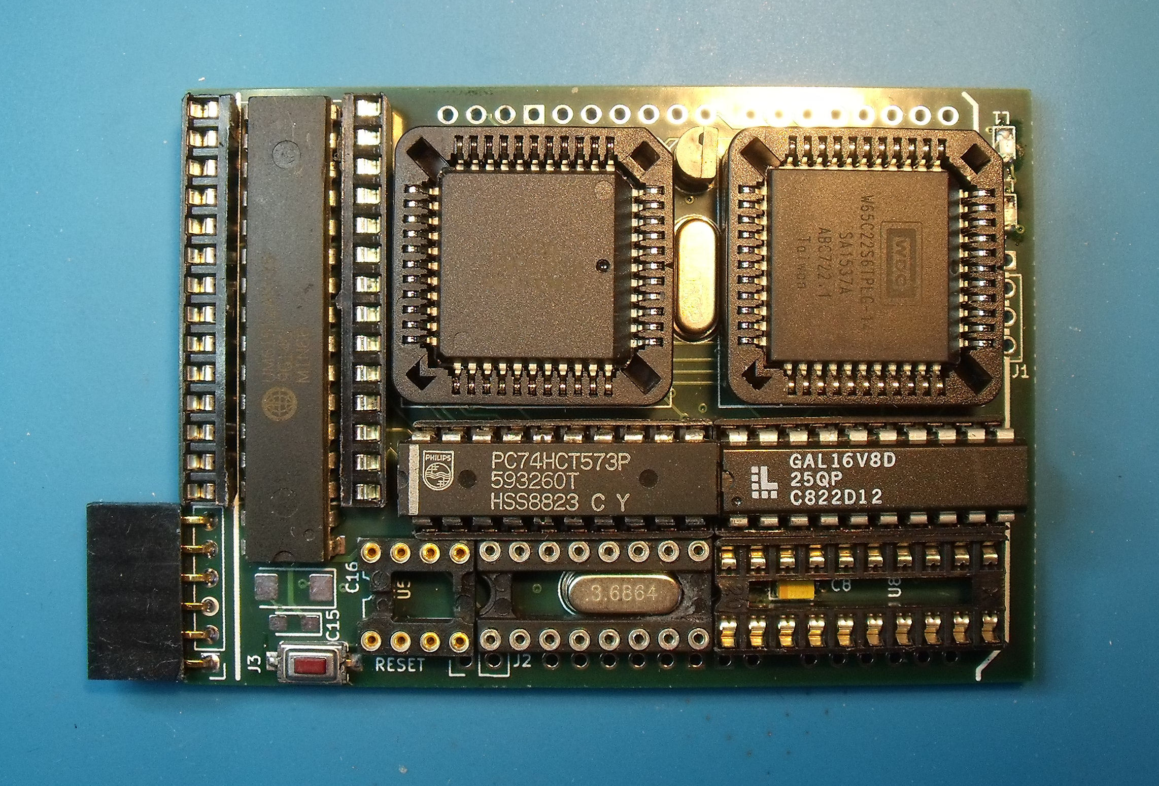
There's so little space on this board that a GAL seemed the logical choice to handle the usual discrete logic. The GAL does address and i/o decoding as follows:
In addition, the GAL inverts the SCC2692 and W65C22S interrupt signals.
Finally, the GAL has the ability to completely switch out the ROM to give access to the full 64K or RAM. The 8085 SOD pin is used to control this feature.
The GAL files are in the code folder.
Below is an image of the pinout I'm using - laid out in a similar way to the Arduino pinout diagrams found on the web. Note that the I2C and SPI signals will hopefully be generated by a software implementation of a hardware interface.
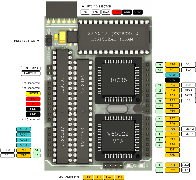
Please see the readme in the Code folder for more details on the software.
The board folder holds the gerber files that were sent to JLCPCB to make the board. It's a 4 layer board but small enough to get it made very cheaply.
The design was done using Kicad 7.0. I'm not sure exactly which files I need to share for the schematic and board layout so I've put the .kicad_pro, .kicad_sch & .kicad_sch files into the board folder. There's also the BOM as a CSV file showing the components used.
Yep, there are errors with v1.2. So far:
| Qty | Value | Footprint | References |
|---|---|---|---|
| 9 | 100n | Capacitor_SMD:C_0603_1608Metric_Pad1.08x0.95mm_HandSolder | C1, C2, C3, C4, C5, C6, C7, C9, C14 |
| 4 | 22p | Capacitor_SMD:C_0603_1608Metric_Pad1.08x0.95mm_HandSolder | C10, C11, C12, C13 |
| 3 | 10K | Resistor_SMD:R_0805_2012Metric_Pad1.20x1.40mm_HandSolder | R1, R2, R12 |
| 2 | 1K | Resistor_SMD:R_0805_2012Metric_Pad1.20x1.40mm_HandSolder | R9, R10 |
| 2 | 4K7 | Resistor_SMD:R_0805_2012Metric_Pad1.20x1.40mm_HandSolder | R7, R8 |
| 2 | LED | LED_SMD:LED_0805_2012Metric_Pad1.15x1.40mm_HandSolder | D2, D3 |
| 1 | 10u | Capacitor_Tantalum_SMD:CP_EIA-3216-18_Kemet-A | C8 |
| 1 | 10u | Capacitor_Tantalum_SMD:CP_EIA-3216-18_Kemet-A_Pad1.58x1.35mm_HandSolder | C15 |
| 1 | 14.7456MHz | Crystal:Crystal_HC49-U_Vertical | Y1 |
| 1 | 22u | Capacitor_Tantalum_SMD:CP_EIA-6032-28_Kemet-C | C16 |
| 1 | 3.6864MHz | Crystal:Crystal_HC49-U_Vertical | Y2 |
| 1 | 74LS573 | Package_DIP:DIP-20_W7.62mm | U2 |
| 1 | ADC0844 | Package_DIP:DIP-20_W7.62mm | U8 |
| 1 | AMS1117-3.3 | Package_TO_SOT_SMD:SOT-223-3_TabPin2 | U10 |
| 1 | Arduino_Uno_R3_Shield | MyLibrary2023:Arduino_Uno_8085_Base_1 | A1 |
| 1 | Conn_01x04 | Connector_PinHeader_2.54mm:PinHeader_1x04_P2.54mm_Vertical | J1 |
| 1 | DS1233-10 | Package_TO_SOT_THT:TO-92L_Inline | U9 |
| 1 | GAL16V8 | Package_DIP:DIP-20_W7.62mm | U3 |
| 1 | MSM80C85AH | Package_LCC:PLCC-44_THT-Socket | U1 |
| 1 | SCC2691AC1N24 | Package_DIP:DIP-24_W7.62mm | U5 |
| 1 | SW_Push | MyLibrary2023:TACTILE_SWITCH_SMD_6.0X3.5MM | SW1 |
| 1 | UM61512AK | Package_DIP:DIP-32_W7.62mm | U6 |
| 1 | W27C512 | Package_DIP:DIP-28_W15.24mm | U7 |
| 1 | W65C22x6TPL | Package_LCC:PLCC-44_THT-Socket | U4 |
| 1 | ~ | Connector_PinHeader_2.54mm:PinHeader_1x06_P2.54mm_Vertical | J3 |
| 1 | ~ | Connector_PinHeader_2.54mm:PinHeader_1x02_P2.54mm_Vertical | J2 |
It measures 76.2 × 53.3 mm and has 4 copper layers, 1.6 mm thick.
42 parts, built around the 74LS573PC, AMS1117-3.3, DS1233-10+T&R and W27C512-45Z. The full list of its parts is on this page, with links to each part's symbol and footprint where PCBKit's library has them.
From the MarkD833/RetroDuino-8085 repository on GitHub, at the commit this page was made from: the board is board/0025_8085_UNO_Board_W65C22_v2.kicad_pcb and its schematic board/0025_8085_UNO_Board_W65C22_v2.kicad_sch. PCBKit opens the board in the browser, with nothing to install.
Its repository publishes it under the GPL-3.0 licence: you may reuse it on that licence's terms (keep the author's notice, and for a copyleft licence share your changes alike).
MarkD833/RCBUS-68xxx
My Motorola 68000 & 68302 processors (+ SIO, PIO & MFP boards) for the RCBus ecosystem.

roberto314/EVA-1_Reproduction
Recreation of the very rare K-K Systems EVA-1 Display Adapter for the Epson HX-20 Computer

SukkoPera/OldPromAdapter
Replace 82s126/82s129/82s131 PROMs with (E)EPROMs


alvaroalea/QL_QsoundQprint_clone
A clone board of the Sound card for the Sinclair QL Computer.


alvaroalea/QL_Minerva_MK2
Clone of the Board of ROM + RTC for Sinclair QL Computer

msx-solis/MSX-EEPROM-Cartridge-64k-v3
Simple MSX ROM cartridge up to 64k