
4 layers58.3 × 32 mm

Carrier PCB for the protocol-emulator demo bench: Icepi Zero, two Picos and every part the demos use
Carrier is an open-source printed circuit board by MarcosAsh, from the MarcosAsh/protocol-emulator-bench repository on GitHub, published under the CERN-OHL-P-2.0 licence. It is a 2-layer board of 100 × 100 mm with 65 parts on 47 nets, routed with 665 tracks and 224 vias.
It is built around the 74AHCT125D, DS18B20 and M2.5. Its parts include 19 resistors, 17 connectors, 5 capacitors, 3 ICs and 3 diodes. It belongs with the RP2040 boards of this library.


The carrier board for the protocol-emulator demo bench. An Icepi Zero (ECP5) plays the chip and two Raspberry Pi Picos drive and check it. The board wires them to every outside part the demos use: two CAN transceivers, an I2C EEPROM, a DS18B20, SPI flash, a NeoPixel stick, SWD into the second Pico, 10BASE-T and two logic analysers.
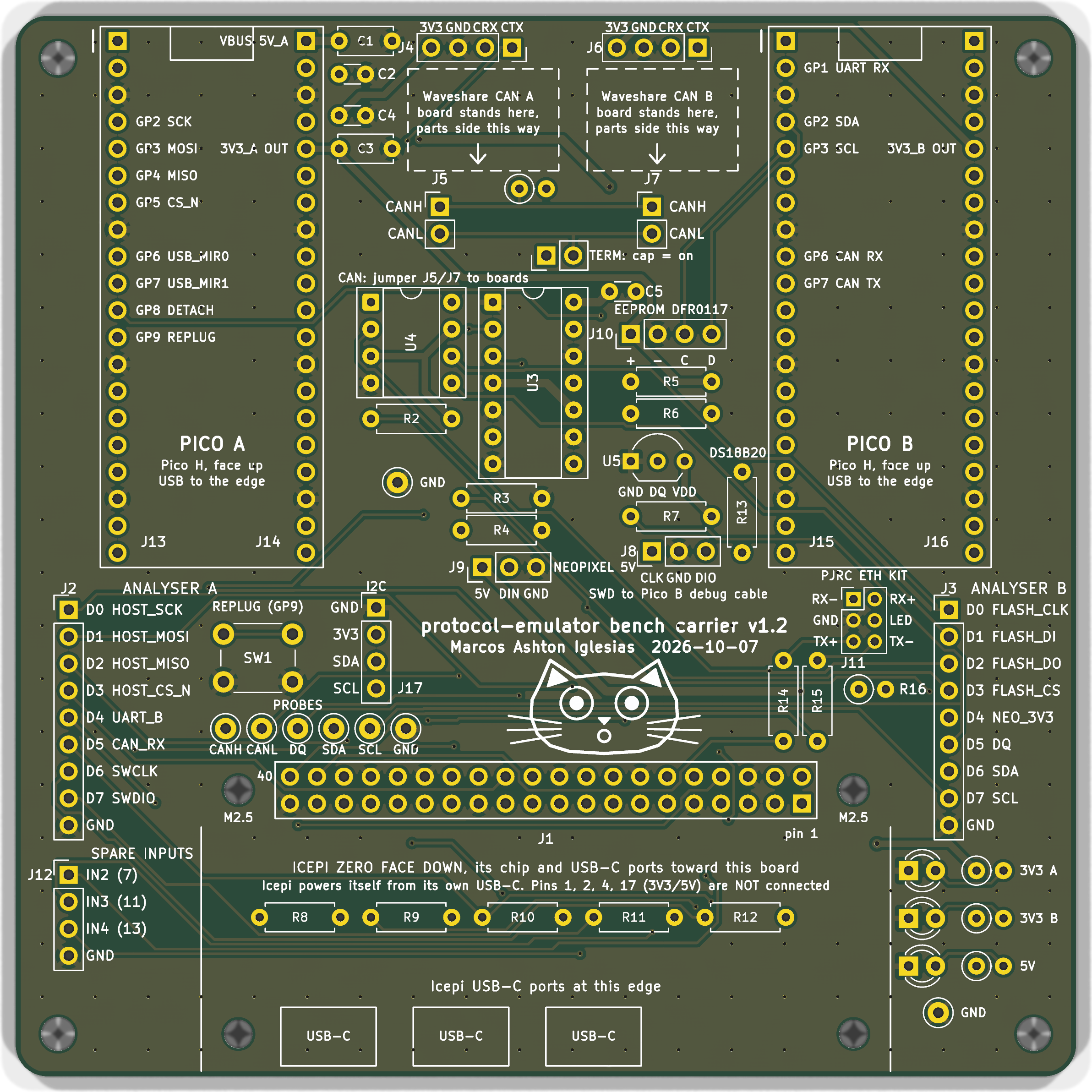
v1.2, 100 x 100 mm, two layers, all through-hole, 47 nets, DRC clean. JLCPCB made and assembled it in
October 2026. The main repo's demo/carrier_check.sh tests every net it can reach on an assembled
board.
| Path | What |
|---|---|
carrier/gen.py | builds the whole board from its parts and nets tables, then routes, checks and plots it |
carrier/carrier.kicad_pcb | the board, KiCad 9 |
carrier/netlist.csv, carrier/bom.csv | nets by pad, and the parts list with what you plug in yourself |
carrier/carrier_jlcpcb_gerbers.zip | gerbers and drills, as ordered |
carrier/jlcpcb/ | JLC assembly BOM and placement files as ordered, and the note on what you fit after delivery |
carrier/renders/ | top and bottom renders and each layer |
Upload carrier_jlcpcb_gerbers.zip to JLCPCB, then jlcpcb/jlc_bom.csv and jlcpcb/jlc_cpl.csv for
through-hole assembly. Check pin 1 of J1, J13-J16, U3, U4 and U5 in their placement preview.
jlcpcb/assembly_note.txt lists the boards and parts that plug in afterwards.
Needs KiCad 9 and its Python module on Linux. From carrier/, python3 gen.py rebuilds everything and
keeps the saved routing while placement and nets are unchanged. python3 gen.py --reroute routes again
with Freerouting, which it expects at tools/freerouting.jar.
CERN-OHL-P v2, see LICENSE.
| Qty | Value | Footprint | References |
|---|---|---|---|
| 4 | M2.5 | MountingHole:MountingHole_2.7mm_M2.5 | H5, H6, H7, H8 |
| 4 | M3 | MountingHole:MountingHole_3.2mm_M3 | H1, H2, H3, H4 |
| 3 | 100n | Capacitor_THT:C_Disc_D3.0mm_W1.6mm_P2.50mm | C2, C4, C5 |
| 3 | 1k | Resistor_THT:R_Axial_DIN0207_L6.3mm_D2.5mm_P7.62mm_Horizontal | R8, R9, R10 |
| 3 | 1k | Resistor_THT:R_Axial_DIN0207_L6.3mm_D2.5mm_P2.54mm_Vertical | R17, R18, R19 |
| 3 | GND | TestPoint:TestPoint_Keystone_5000-5004_Miniature | TP1, TP2, TP3 |
| 2 | 10k | Resistor_THT:R_Axial_DIN0207_L6.3mm_D2.5mm_P7.62mm_Horizontal | R2, R3 |
| 2 | 10u | Capacitor_THT:C_Disc_D5.0mm_W2.5mm_P5.00mm | C1, C3 |
| 2 | 220R | Resistor_THT:R_Axial_DIN0207_L6.3mm_D2.5mm_P7.62mm_Horizontal | R11, R12 |
| 2 | 2k2 | Resistor_THT:R_Axial_DIN0207_L6.3mm_D2.5mm_P7.62mm_Horizontal | R5, R6 |
| 2 | 47R | Resistor_THT:R_Axial_DIN0207_L6.3mm_D2.5mm_P7.62mm_Horizontal | R14, R15 |
| 2 | 4k7 | Resistor_THT:R_Axial_DIN0207_L6.3mm_D2.5mm_P7.62mm_Horizontal | R7, R13 |
| 2 | green | LED_THT:LED_D3.0mm | D1, D2 |
| 1 | 120R | Resistor_THT:R_Axial_DIN0207_L6.3mm_D2.5mm_P2.54mm_Vertical | R1 |
| 1 | 330R | Resistor_THT:R_Axial_DIN0207_L6.3mm_D2.5mm_P7.62mm_Horizontal | R4 |
| 1 | 470R | Resistor_THT:R_Axial_DIN0207_L6.3mm_D2.5mm_P2.54mm_Vertical | R16 |
| 1 | 74AHCT125 | Package_DIP:DIP-14_W7.62mm_Socket | U3 |
| 1 | ANALYSER A | Connector_PinHeader_2.54mm:PinHeader_1x09_P2.54mm_Vertical | J2 |
| 1 | ANALYSER B | Connector_PinHeader_2.54mm:PinHeader_1x09_P2.54mm_Vertical | J3 |
| 1 | CAN A | Connector_PinSocket_2.54mm:PinSocket_1x04_P2.54mm_Vertical | J4 |
| 1 | CAN A BUS | Connector_PinHeader_2.54mm:PinHeader_1x02_P2.54mm_Vertical | J5 |
| 1 | CAN B | Connector_PinSocket_2.54mm:PinSocket_1x04_P2.54mm_Vertical | J6 |
| 1 | CAN B BUS | Connector_PinHeader_2.54mm:PinHeader_1x02_P2.54mm_Vertical | J7 |
| 1 | CANH | TestPoint:TestPoint_Keystone_5000-5004_Miniature | TP4 |
| 1 | CANL | TestPoint:TestPoint_Keystone_5000-5004_Miniature | TP5 |
| 1 | DQ | TestPoint:TestPoint_Keystone_5000-5004_Miniature | TP6 |
| 1 | DS18B20 | Package_TO_SOT_THT:TO-92_Inline_Wide | U5 |
| 1 | EEPROM | Connector_PinHeader_2.54mm:PinHeader_1x04_P2.54mm_Vertical | J10 |
| 1 | ETHERNET | Connector_PinHeader_2.00mm:PinHeader_2x03_P2.00mm_Vertical | J11 |
| 1 | I2C | Connector_PinHeader_2.54mm:PinHeader_1x04_P2.54mm_Vertical | J17 |
| 1 | Icepi Zero | carrier:IcepiZero_Socket_2x20_FaceDown | J1 |
| 1 | NEOPIXEL | Connector_PinHeader_2.54mm:PinHeader_1x03_P2.54mm_Vertical | J9 |
| 1 | Pico A left | carrier:PinSocket_1x20_P2.54mm_Vertical_NoSilk | J13 |
| 1 | Pico A right | carrier:PinSocket_1x20_P2.54mm_Vertical_NoSilk | J14 |
| 1 | Pico B left | carrier:PinSocket_1x20_P2.54mm_Vertical_NoSilk | J15 |
| 1 | Pico B right | carrier:PinSocket_1x20_P2.54mm_Vertical_NoSilk | J16 |
| 1 | REPLUG | Button_Switch_THT:SW_PUSH_6mm | SW1 |
| 1 | SCL | TestPoint:TestPoint_Keystone_5000-5004_Miniature | TP8 |
| 1 | SDA | TestPoint:TestPoint_Keystone_5000-5004_Miniature | TP7 |
| 1 | SPARE | Connector_PinHeader_2.54mm:PinHeader_1x04_P2.54mm_Vertical | J12 |
| 1 | SWD | Connector_PinHeader_2.54mm:PinHeader_1x03_P2.54mm_Vertical | J8 |
| 1 | TERM | Connector_PinHeader_2.54mm:PinHeader_1x02_P2.54mm_Vertical | JP1 |
| 1 | W25Q64 breakout | Package_DIP:DIP-8_W7.62mm_Socket | U4 |
| 1 | red | LED_THT:LED_D3.0mm | D3 |
It measures 100 × 100 mm and has 2 copper layers, 1.6 mm thick.
65 parts, built around the 74AHCT125D, DS18B20 and M2.5. The full list of its parts is on this page, with links to each part's symbol and footprint where PCBKit's library has them.
From the MarcosAsh/protocol-emulator-bench repository on GitHub, at the commit this page was made from: the board is carrier/carrier.kicad_pcb. PCBKit opens the board in the browser, with nothing to install.
Its repository publishes it under the CERN-OHL-P-2.0 licence: you may reuse it on that licence's terms (keep the author's notice, and for a copyleft licence share your changes alike).


klaus-liebler/sensact
Es gibt vier Namespaces für Nachrichten "REQUEST" und "RESPONSE", "EVENT" und "ACKNOWLEDGE". Dies wird mit den beiden LSB des Versions-Namespace-Bytes erklärt (Somit bleiben 64 Versionierungsmöglichkeiten) Alle vier…


byungyoonc/TrueStrike42
TrueStrike42 is a columnar staggered unibody split keyboard designed to maximize performance and minimize finger fatigue.

twasilczyk/waterdrop-esphome
Waterdrop RO system smart Wi-Fi module for Home Assistant