Educational KiCad power-supply examples demonstrating linear regulation, buck/boost conversion and current limiting, with design trade-offs and improvement notes.
Voltage Regulator seneryo Y (Input 3.7V) is an open-source printed circuit board by manyetox, from the manyetox/Voltage-Regulator-Examples repository on GitHub. It is a 2-layer board of 50 × 50 mm with 43 parts on 33 nets, routed with 379 tracks and 26 vias.
It is built around the MC33063AD and 1N5819WS. Its parts include 21 resistors, 13 capacitors, 4 ICs, 2 diodes and 2 inductors. It belongs with the power boards of this library.
Voltage Regulator Examples — Linear, Buck, Boost & Current Limiting
A small educational PCB project exploring several common ways of generating and controlling power rails.
The repository contains two 50 × 50 mm, 2-layer KiCad boards built around different input-voltage scenarios:
15 V input version — demonstrates a fixed linear regulator, an LM2596 buck converter, a TL317-based regulation/current-limiting stage, and a TL071 control section.
3.7 V input version — demonstrates MC33063 switching-converter stages together with TL317 current-limited outputs.
The project is useful as a learning example because it puts several classic power-supply techniques next to each other rather than hiding everything inside one modern power-management IC.
Important: This repository is best treated as an educational/reference design. Before using either board in a real product, re-check the exact component part numbers, footprints, thermal limits, current ratings, input range, output ripple, and switching layout.
What Is a Voltage Regulator?
Electronic circuits normally need a reasonably stable supply voltage.
A battery or external supply is rarely perfect:
its voltage changes with load;
battery voltage changes as the battery discharges;
motors and radios can create current spikes;
different parts of a system may require different voltages.
A voltage regulator converts an available supply into a rail that is more suitable for the load.
For example:
text
15 V input
   |
   +----> 12 V regulator ----> 12 V load
   |
   +----> 5 V regulator -----> 5 V load
There are several ways to do this, and each has different advantages.
This project intentionally contains several of them.
1. Linear vs Switching Regulators
Linear regulator
A linear regulator behaves approximately like a controlled variable resistance.
text
Higher voltage
     |
     v
+-----------+
|  Linear   |
| Regulator |
+-----------+
     |
     v
Lower regulated voltage
Its biggest advantage is simplicity.
Typical advantages:
few external components;
low switching noise;
easy to understand;
often inexpensive.
The main disadvantage is that the unused voltage is converted into heat.
The approximate regulator dissipation is:
text
P_loss ≈ (V_in - V_out) × I_out
That makes a linear regulator attractive when the voltage difference and current are both small, but inefficient when a large voltage drop is required.
Switching regulator
A switching regulator rapidly switches current through an inductor and controls the average energy transferred to the output.
Rather than continuously burning the excess voltage as heat, it stores and transfers energy.
This can provide much better efficiency.
The trade-offs are:
more components;
more complicated PCB layout;
switching ripple;
electromagnetic interference;
component-selection requirements;
control-loop and transient considerations.
The switching regulator is usually the better choice when efficiency matters or when the output must be higher than the input.
2. Buck and Boost Converters
Buck converter
A buck converter produces a voltage lower than its input.
text
15 V
 |
 v
+------+
| BUCK |
+------+
 |
 v
5 V
The 15 V version of this project uses an LM2596S-ADJ switching regulator as a buck-converter stage.
The LM2596 is a classic asynchronous switching regulator operating at 150 kHz and capable of relatively high output current when designed and cooled correctly.
Boost converter
A boost converter produces a voltage higher than its input.
text
3.7 V
  |
  v
+-------+
| BOOST |
+-------+
  |
  v
Higher voltage
This is useful when a low-voltage battery needs to power a circuit that requires a higher rail.
The 3.7 V design uses MC33063A switching-regulator ICs.
The MC33063 can be configured as:
buck;
boost;
inverting converter.
This flexibility is one reason it is useful for learning power-electronics fundamentals.
3. Why Inductors Are Used
An inductor stores energy in a magnetic field.
A switching regulator repeatedly performs something similar to:
text
Switch ON
   |
   v
Inductor stores energy

Switch OFF
   |
   v
Inductor releases energy into the load
The controller adjusts this process so the output stays near the requested voltage.
The required inductance depends on factors including:
input voltage;
output voltage;
load current;
switching frequency;
desired ripple current.
Older, lower-frequency converters usually require physically larger inductors.
That can be seen clearly in the 3.7 V version of this project, which uses 330 µH inductors.
4. Why the Diode Is Needed
The switching stages use 1N5819-class Schottky diodes.
When the internal switch turns off, the inductor current cannot instantly become zero.
The diode gives that current a path to continue flowing.
Schottky diodes are traditionally used in converters like these because they have:
relatively low forward voltage;
fast switching behavior.
In a modern synchronous converter, a MOSFET often replaces this diode to improve efficiency.
5. Why Large Output Capacitors Are Used
A switching regulator does not deliver perfectly smooth DC directly from the switch node.
The output capacitor stores charge and supplies the load between switching events.
It therefore helps reduce:
output ripple;
transient voltage movement;
short load-step disturbances.
The 3.7 V design uses several 330 µF electrolytic capacitors.
These values are relatively large because the MC33063 operates at a comparatively low switching frequency.
Modern high-frequency converters can often achieve similar performance using much smaller inductors and capacitors.
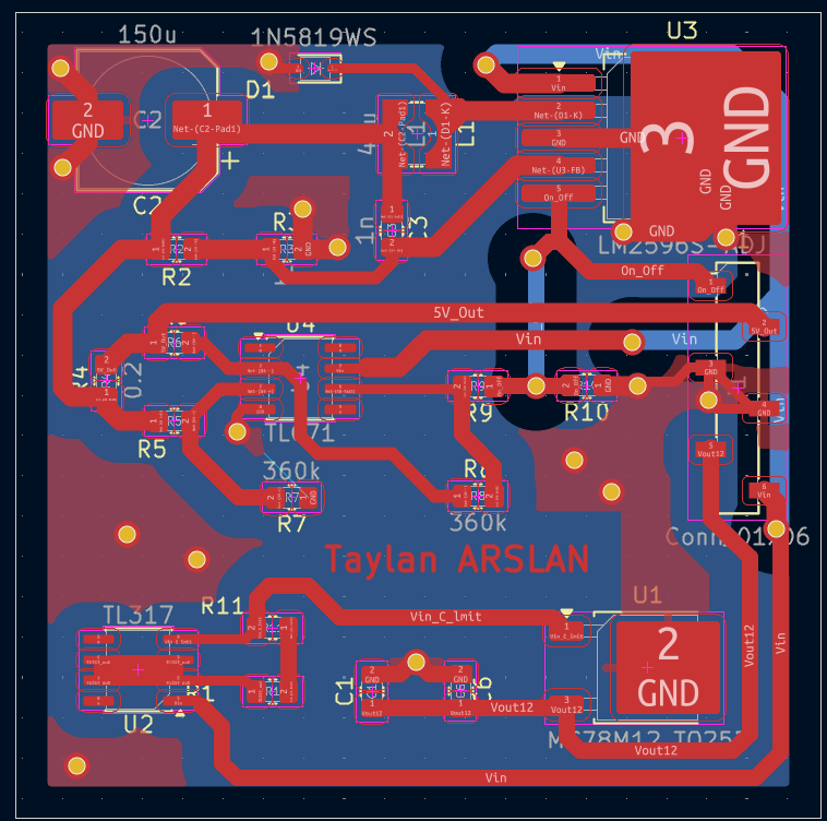
6. 15 V Input Version
The 15 V design contains several different regulator approaches on the same PCB.
PCB layout
15 V input board layout. This board deliberately places multiple regulator approaches on one compact PCB so their implementation can be compared directly.
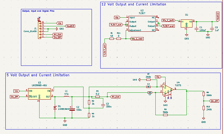
Schematic
Complete schematic of the 15 V input version. The fixed linear, switching, current-regulation, and analog-control sections can be followed independently.
Main devices:
Reference
Device
Purpose
U1
MC78M12
Fixed 12 V linear regulator
U2
TL317
Adjustable linear/current-regulator section
U3
LM2596S-ADJ
Switching buck regulator
U4
TL071
Analog control / conditioning section
The board is approximately:
text
50 mm × 50 mm
2 copper layers
6.1 MC78M12 — fixed 12 V linear regulator
The MC78M12 is a classic fixed positive linear regulator.
Its job is conceptually simple:
text
Vin
 |
 v
+---------+
| MC78M12 |
+---------+
 |
 v
12 V
The main advantage is simplicity.
There is no switching node, external inductor, feedback-divider design, or high-frequency power loop.
Why it is useful educationally
It demonstrates the simplest form of voltage regulation.
You can compare it directly with the switching-regulator section and observe the differences in:
complexity;
temperature;
ripple;
efficiency;
component count.
Limitation
The MC78M12 needs voltage headroom above 12 V in order to remain regulated.
A nominal 15 V input therefore does not provide a huge amount of margin if the source voltage falls.
It also dissipates the voltage difference as heat:
text
P_loss ≈ (Vin - 12 V) × Iout
For significant current, thermal design becomes important.
6.2 LM2596 — 5 V switching stage
The board also contains an LM2596S-ADJ.
The LM2596 is a classic 150 kHz buck regulator.
Unlike the 78M12, it transfers energy through an inductor instead of intentionally dropping the excess voltage across a pass transistor.
Conceptually:
text
15 V
 |
 v
+---------+
| LM2596  |
|  BUCK   |
+---------+
 |
 v
5 V
The board exposes the result as:
text
5V_Out
Why this is a better topology for 15 V → 5 V
Dropping 15 V directly to 5 V with a linear regulator wastes a large portion of the input power as heat.
A buck regulator is normally far more appropriate when:
the voltage difference is large;
output current is significant;
efficiency matters.
6.3 Inductor and Schottky diode
The LM2596 stage uses:
L1 = 47 µH
D1 = 1N5819WS-class Schottky diode
a large output capacitor.
These parts form the external power path around the regulator.
The switching-current loop is one of the most important parts of any buck-converter PCB.
It should be:
short;
compact;
wide enough for the expected current;
located close to the regulator and diode.
6.4 ON/OFF control
The 15 V board exposes an:
text
On_Off
signal on its external connector.
This is useful because a switching regulator does not necessarily need to run continuously.
An enable/shutdown input can:
reduce standby consumption;
allow sequencing;
let a microcontroller control the rail.
6.5 TL317 section
The TL317 is an adjustable low-current linear regulator.
It can also be configured as a precision current limiter.
In current-regulator form, the basic relationship is:
text
I_limit ≈ 1.25 V / R_set
This is a useful teaching circuit because it shows that a regulator can control current, not only voltage.
The schematic contains a 43 Ω resistor, which appears to be associated with the TL317/current-limiting section.
Before relying on a specific limit value, verify the exact schematic connectivity and resistor tolerance.
Important limitation
The TL317 is a low-current device.
It is useful for:
small loads;
current-limited experiments;
LEDs;
reference circuits;
learning current regulation.
It is not a suitable replacement for a high-current power-stage current limiter.
6.6 TL071 analog section
The 15 V design also contains a TL071 JFET-input operational amplifier.
This is a classic analog op-amp and can be useful for:
sensing;
amplification;
control;
threshold-related analog circuitry.
However, the TL071 is not rail-to-rail.
That matters in single-supply circuits.
Signals very close to ground or the positive supply may fall outside its comfortable input/output operating range.
For a new modern design, I would normally consider a rail-to-rail op-amp or a dedicated comparator if the job is simply threshold detection.
6.7 15 V board connector
The PCB routes J1 as:
J1 pin
Net
1
On_Off
2
5V_Out
3
GND
4
GND
5
Vout12
6
Vin
This gives the board one input supply, two ground pins, two regulated rails, and one control signal.
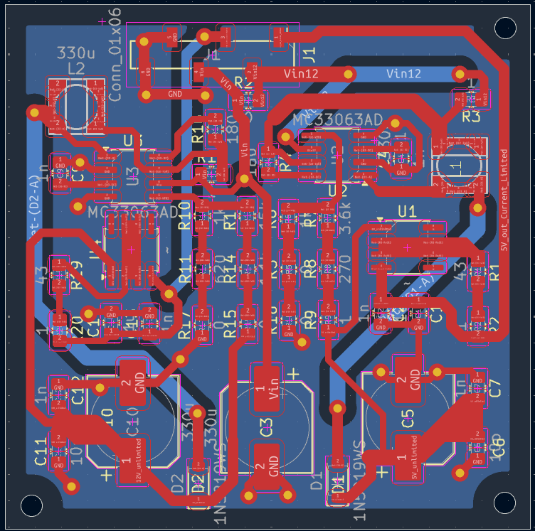
7. 3.7 V Input Version
The second board explores a different problem:
What if the available voltage is low and a higher rail is required?
PCB layout
3.7 V input board layout. The larger inductors and electrolytic capacitors make the physical consequences of a low-frequency switching-converter design easy to see.
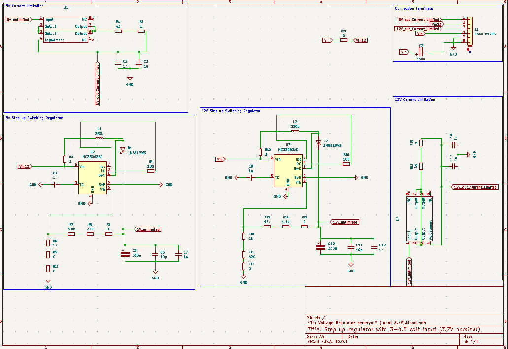
Schematic
Complete schematic of the 3.7 V input version, showing the MC33063 conversion stages and the following TL317 current-limiting sections.
The design uses two MC33063AD converter stages and two TL317-based current-limiting stages.
The main component set includes:
2 × MC33063AD;
2 × TL317;
2 × 330 µH inductors;
2 × Schottky diodes;
several 330 µF capacitors.
The board is also:
text
50 mm × 50 mm
2 copper layers
7.1 MC33063 converter
The MC33063 is a classic switching-regulator controller with an internal power switch.
It can implement several basic converter topologies.
Its main educational value is that many of the power-converter design decisions are visible externally:
timing capacitor;
current-sense resistor;
inductor;
catch diode;
feedback divider;
output capacitor.
A highly integrated modern converter hides more of this.
7.2 Feedback divider
A switching regulator must know whether its output voltage is too high or too low.
Good net names are part of good electrical documentation.
8. What Was Done Well
Even though several component choices are old-fashioned by modern power-supply standards, the project has good educational qualities.
Multiple regulator types on real PCBs
Instead of only showing theory, the project contains actual layouts for:
fixed linear regulation;
adjustable linear regulation;
current regulation;
buck conversion;
boost conversion.
That makes it useful for comparing technologies directly.
The power stages are visible
The inductor, diode, output capacitor, current-sense resistors, and feedback network are all visible as separate parts.
This makes it much easier to learn what each component actually does.
Separate grounds are provided on the connector
Using two ground pins on the six-pin interface makes bench testing easier and gives more convenient return connections.
KiCad source and BOM files are included
The repository is not only a picture of a finished PCB.
It contains editable design files, which means someone can:
inspect the schematic;
measure the PCB;
change values;
regenerate manufacturing files;
use it as a starting point for another design.
9. What Is Suboptimal?
This is the most useful part of the project from an educational perspective.
A circuit can work and still not be the way you would design a new commercial product.
9.1 MC33063 is very old and low-frequency
The MC33063 is excellent for learning because its operation is easy to see.
It is less attractive for a modern compact design.
Its switching frequency is relatively low, which is one reason this board needs:
text
330 µH inductors
330 µF electrolytic capacitors
A modern synchronous converter running at a much higher frequency could usually achieve the same basic job with:
a much smaller inductor;
much smaller capacitors;
higher efficiency;
smaller PCB area.
Better modern approach
For a production design, select a modern synchronous buck/boost IC specifically for the required:
input range;
output voltage;
output current;
efficiency;
package size.
9.2 Boosting from a nominal 3.7 V source needs proper battery-range analysis
If the 3.7 V input represents a lithium battery, 3.7 V is only the nominal voltage.
The converter must be designed for the complete operating range of the source, not one nominal value.
Important checks include:
startup at the lowest allowed battery voltage;
peak switch current;
input current at maximum boost ratio;
battery internal resistance;
undervoltage protection.
The MC33063 itself has a minimum operating-input requirement, so operating close to the bottom of a battery's usable range needs particular attention.
9.3 MC78M12 wastes power as heat
The 12 V rail on the 15 V version uses a linear regulator.
That is simple, but:
text
Power loss = voltage dropped × load current
As current increases, the regulator gets hotter.
A switching buck regulator would be more efficient.
When the linear regulator still makes sense
It is still useful when:
current is low;
simplicity matters;
low switching noise matters;
the voltage difference is small.
For an educational comparison board, this is a perfectly reasonable part to include.
9.4 The 15 V → 12 V regulator has limited headroom
The MC78M12 needs the input to stay sufficiently above 12 V.
A nominal 15 V supply works, but there is not enormous margin if:
the input supply sags;
a cable drops voltage;
the source is a battery;
load current increases.
A lower-dropout regulator would give more operating margin.
9.5 TL317 is limited to small currents
The TL317 is useful for demonstrating adjustable voltage and precision current limiting, but it is not a high-current regulator.
For larger loads, a better design would use:
a dedicated current-limit IC;
an eFuse;
a load switch with programmable current limit;
a switching converter with current regulation;
a MOSFET-based current controller.
9.6 TL071 is not ideal for low-voltage single-supply work
The TL071 is a classic and useful op-amp, but it was not designed as a modern rail-to-rail device.
If the circuit being monitored approaches ground, the op-amp input/output range becomes important.
A modern design would select the amplifier based on:
input common-mode range;
rail-to-rail requirement;
output swing;
offset voltage;
supply voltage;
bandwidth.
If the circuit only needs threshold detection, use a comparator rather than an op-amp.
9.7 Exact component specifications are incomplete
Several BOM entries describe only a value.
Examples include:
text
330 µH
330 µF
1 µF
For a power converter, the value alone is not enough.
Inductor specification should include
inductance;
saturation current;
RMS current;
DCR;
tolerance;
package;
manufacturer part number.
Capacitor specification should include
capacitance;
voltage rating;
ESR;
ripple-current rating;
tolerance;
temperature rating;
manufacturer part number.
Without these, two components with the same printed value can behave very differently.
9.8 The Schottky diode footprint should be rechecked
In the 3.7 V project, D1 and D2 are labelled:
text
1N5819WS
but the BOM points to a SOD-123 footprint.
1N5819W and 1N5819WS naming is not always used consistently across manufacturers, but the WS suffix is commonly associated with a smaller package.
Before manufacturing another board:
verify the exact manufacturer part number against the actual footprint.
Never choose a diode footprint based only on the generic 1N5819 family name.
9.9 More ceramic decoupling should be considered
Switching and analog ICs generally benefit from small ceramic bypass capacitors placed immediately beside their supply pins.
A future revision should compare every IC with its datasheet-recommended input/output bypassing.
As a general design habit:
text
large capacitor = lower-frequency energy storage
small ceramic capacitor = high-frequency local decoupling
Both can be necessary.
9.10 Protection could be improved
For a bench example, a bare input can be acceptable.
For a real system I would consider adding:
input fuse or resettable fuse;
reverse-polarity protection;
transient-voltage suppression;
overvoltage protection;
undervoltage lockout;
output short-circuit strategy;
test points.
9.11 PCB power loops should be kept very small
Switching-regulator performance depends on PCB layout, not only the schematic.
The highest-current switching loop should be compact.
For an asynchronous converter, this normally includes the:
regulator switch;
diode;
inductor;
input/output capacitors;
ground return.
Long thin traces increase:
parasitic inductance;
ringing;
EMI;
voltage spikes;
loss.
A future revision should be laid out directly from the manufacturer's recommended layout rather than arranging components primarily for visual symmetry.
9.12 0805 current-sense resistors need a power check
Very low-value resistors in a switching regulator can carry significant pulsed current.
The resistance may be small, but the power is:
text
P = I²R
The pulse rating can matter as much as average power.
For high-current paths, consider:
appropriately rated current-sense resistors;
Kelvin connections;
wider copper;
larger packages where necessary.
10. How I Would Redesign It Today
For a modern compact board I would probably use:
text
Low-voltage source
        |
        v
Modern synchronous boost / buck-boost converter
        |
        +----> main regulated rail
        |
        +----> modern synchronous buck
                    |
                    +----> lower-voltage rail
For current-limited outputs:
text
Regulated rail
      |
      v
eFuse / programmable load switch
      |
      v
Protected output
I would also add:
exact manufacturer part numbers;
input reverse-polarity protection;
fuse/eFuse;
test points;
power LEDs if useful;
clear connector labels;
ground plane;
local 100 nF decoupling;
thermal copper around hot devices;
measurement points for switch node and feedback;
a documented maximum load for every output.
The resulting PCB could be much smaller than 50 × 50 mm.
However, it would also hide more of the basic converter behavior.
That is why the existing design remains useful as a teaching board.
11. Suggested Experiments
This project becomes much more educational when used with a bench supply, electronic load, oscilloscope, and multimeter.
Experiment 1 — line regulation
Change the input voltage and measure:
text
Vout vs Vin
Observe when each regulator stops maintaining its intended output.
Experiment 2 — load regulation
Increase output current gradually and measure:
text
Vout vs Iout
Compare the linear and switching stages.
Experiment 3 — thermal behavior
Measure regulator temperature at several load currents.
Compare:
MC78M12;
LM2596;
TL317.
This demonstrates why efficiency matters.
Experiment 4 — switching ripple
Use an oscilloscope to inspect the switching-regulator output.
Measure:
switching frequency;
ripple amplitude;
transient response.
Use a short ground spring on the oscilloscope probe for meaningful high-frequency measurements.
Experiment 5 — efficiency
Measure:
text
P_in  = V_in × I_in
P_out = V_out × I_out
Then:
text
Efficiency = P_out / P_in
Compare the linear and switching regulators.
Experiment 6 — current limiting
Use an electronic load or a suitable resistor load and slowly increase current.
Observe the TL317 current-limiter behavior.
Do not intentionally short an output unless the circuit and load source have been verified safe for that test.
12. Repository Structure
The archive currently contains two main project folders:
text
Voltage Regulator example simple/
│
├── Media/
│   ├── 15V input layout.png
│   ├── 15V input schematic.png
│   ├── 3.7V layout.png
│   └── 3.7V inut schmatic.png
│
├── Voltage Regulator seneryo Y (Input 15V)/
│   ├── *.kicad_pro
│   ├── *.kicad_sch
│   ├── *.kicad_pcb
│   └── BOM.csv
│
└── Voltage Regulator seneryo Y (Input 3.7V)/
    ├── *.kicad_pro
    ├── *.kicad_sch
    ├── *.kicad_pcb
    ├── BOM.csv
    ├── STEP / WRL model
    └── Gerber/
There are also KiCad autosave, lock, history, and backup files.
For a clean public repository, I recommend removing:
text
*_autosave*
*.lck
*.kicad_prl
*-backups/
after making sure the final source files are safely preserved.
For cleaner long-term links, I would also eventually rename the media files to remove spaces and fix the existing inut schmatic typo. If you do that, update the image links in this README at the same time.
I would also rename:
text
seneryo Y
to something descriptive for an international audience.
Recalculate switching-regulator component values from the current datasheets.
Validate regulator thermal behavior.
Measure ripple under load.
Verify current limiting.
Regenerate Gerbers from the final source revision.
15. Main Lessons From This Project
The most important lesson is that "a voltage regulator" is not one single circuit.
Different problems need different topologies.
Linear regulator
Best when:
simplicity matters;
current is modest;
voltage drop is small;
low switching noise is important.
Buck converter
Best when:
text
Vout < Vin
and efficiency matters.
Boost converter
Best when:
text
Vout > Vin
Current regulator / limiter
Best when the important controlled quantity is current, not simply voltage.
The right design depends on the source, load, thermal budget, noise requirement, size, cost, and efficiency target.
16. Project Status
This repository is published primarily as an educational voltage-regulation example.
It should be useful for:
students learning power electronics;
beginners learning KiCad;
comparing linear and switching regulators;
learning feedback networks;
understanding inductors and Schottky diodes;
studying current limiting;
improving an older regulator design with modern components.
The project is especially valuable because some parts are deliberately simple or old-school enough that the operation can be followed directly from the schematic.
The suboptimal choices are part of the learning value: they show why modern power-supply ICs, careful component specification, and layout discipline matter.
Educational KiCad power-supply examples demonstrating linear regulation, buck/boost conversion and current limiting, with design trade-offs and improvement notes.
What happens when you combine a Woodworker, and an Electrical Engineer? Sometimes the result are things like this. A Mesh controlled set of blast gates for dust collection control.
Diplomarbeit 2024-2025 mit der Firma B2 electronics. Das Ziel ist es eine Sensorbox mit dem ESP32, als Basis zu entwickeln. Diese Sensorbox soll über ein Mesh-Netzwerk erweiterbar werden.
82 parts
Questions
How big is the Voltage Regulator seneryo Y (Input 3.7V) PCB?
It measures 50 × 50 mm and has 2 copper layers, 1.6 mm thick.
What parts does the Voltage Regulator seneryo Y (Input 3.7V) use?
43 parts, built around the MC33063AD and 1N5819WS. The full list of its parts is on this page, with links to each part's symbol and footprint where PCBKit's library has them.
Where can I download the Voltage Regulator seneryo Y (Input 3.7V) KiCad files?
From the manyetox/Voltage-Regulator-Examples repository on GitHub, at the commit this page was made from: the board is Hardware/Voltage Regulator (Input 3.7V)/Voltage Regulator seneryo Y (Input 3.7V).kicad_pcb and its schematic Hardware/Voltage Regulator (Input 15V)/Voltage Regulator seneryo Y (Input 15V).kicad_sch. PCBKit opens the board in the browser, with nothing to install.
Can I use the Voltage Regulator seneryo Y (Input 3.7V) design in my own project?
Its repository states no licence, so its author keeps all rights: ask manyetox before reusing the design.