
2 layers49.6 × 78.3 mm
Odyssey
jotego/jtcores
FPGA cores compatible with multiple arcade game machines and KiCAD schematics of arcade games. Working on MiSTer FPGA/Analogue Pocket
24 parts346GPL-3.0
 Manideep136/Half-Adder
A Half Adder is a basic digital logic circuit used to perform the addition of two single-bit binary numbers. It produces two outputs:
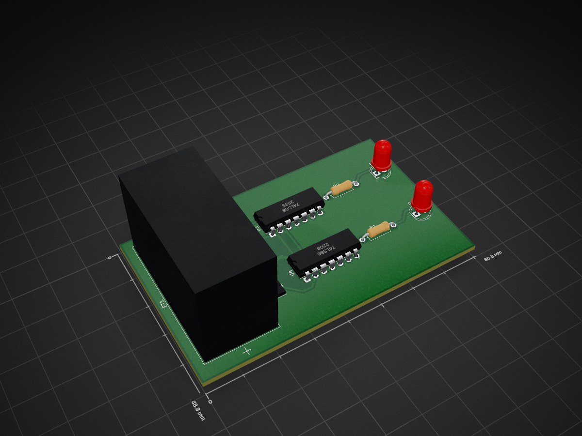
Half Adder is an open-source printed circuit board by Manideep136, from the Manideep136/Half-Adder repository on GitHub. It is a 2-layer board of 80.8 × 48.8 mm with 9 parts on 26 nets, routed with 68 tracks and 0 vias.
It is built around the 74LS86. Its parts include 2 resistors, 2 ICs, 2 diodes and 2 switches.
A Half Adder is a basic digital logic circuit used to perform the addition of two single-bit binary numbers. It produces two outputs:
The Half Adder is one of the fundamental building blocks used in digital electronics and forms the basic concept behind more complex arithmetic circuits such as Full Adders, Binary Adders, and Arithmetic Logic Units (ALUs).
This project demonstrates the design and implementation of a Half Adder circuit using logic gates and a PCB designed using KiCad.
A Half Adder accepts two binary inputs:
It produces:
1The Sum output is generated using an XOR gate, while the Carry output is generated using an AND gate.
Sum = A XOR B

Carry = A AND B
Therefore, the circuit requires:
| A | B | Sum | Carry |
|---|---|---|---|
| 0 | 0 | 0 | 0 |
| 0 | 1 | 1 | 0 |
| 1 | 0 | 1 | 0 |
| 1 | 1 | 0 | 1 |
| Component | Quantity | Purpose |
|---|---|---|
| XOR Gate IC | 1 | Generates Sum |
| AND Gate IC | 1 | Generates Carry |
| LED | 2 | Indicates Sum and Carry |
| Resistors | 2 | Limits LED current |
| Push Buttons/Switches | 2 | Provides inputs A and B |
| Breadboard/PCB | 1 | Circuit implementation |
| Connecting Wires | As required | Electrical connections |
| Power Supply | 1 | Provides circuit power |
For a 74-series implementation, commonly used ICs include:
The two input switches provide binary values A and B.
The inputs are connected simultaneously to the XOR and AND gates.
             ┌─────────────┐
      A ─────┤             │
             │   XOR Gate  ├──── Sum
      B ─────┤             │
             └─────────────┘

             ┌─────────────┐
      A ─────┤             │
             │   AND Gate  ├──── Carry
      B ─────┤             │
             └─────────────┘
When the inputs are different, the XOR gate produces a 1, so the Sum LED turns ON.
When both inputs are 1, the AND gate produces a 1, so the Carry LED turns ON.
The project can be designed using KiCad through the following stages:
The PCB contains the components required to implement the Half Adder circuit.
The board can include:
Proper component placement and routing should be used to keep the PCB compact and easy to understand.
After assembling the PCB, the circuit can be tested by applying all possible combinations of the two inputs.
| Input A | Input B | Expected Sum | Expected Carry |
|---|---|---|---|
| OFF | OFF | OFF | OFF |
| OFF | ON | ON | OFF |
| ON | OFF | ON | OFF |
| ON | ON | OFF | ON |
The observed outputs should match the truth table.
Half Adders are used as basic building blocks in:
A Half Adder can add only two single-bit binary numbers. It does not have a Carry-In input.
Therefore, it cannot directly add multiple-bit binary numbers where a carry from a previous bit needs to be considered. For this purpose, a Full Adder is used.
The project can be extended by:
Manideep
Electronics and Communication Engineering (ECE)
The Half Adder is a fundamental digital logic circuit that demonstrates how binary addition can be implemented using basic logic gates. In this project, an XOR gate is used to generate the Sum, while an AND gate generates the Carry. The circuit provides a simple and practical introduction to digital arithmetic and PCB design.
| Qty | Value | Footprint | References |
|---|---|---|---|
| 2 | 470R | Resistor_THT:R_Axial_DIN0207_L6.3mm_D2.5mm_P10.16mm_Horizontal | R1, R2 |
| 2 | LED | LED_THT:LED_D5.0mm | D1, D2 |
| 2 | SW_Nidec_CAS-120A1 | Button_Switch_SMD:Nidec_Copal_CAS-120A | SW1, SW2 |
| 1 | 74LS08 | Package_DIP:DIP-14_W7.62mm | U3 |
| 1 | 74LS86 | Package_DIP:DIP-14_W7.62mm | U4 |
| 1 | Battery | Battery:BatteryHolder_Bulgin_BX0123_1xCR123 | BT1 |
It measures 80.8 × 48.8 mm and has 2 copper layers, 1.6 mm thick.
9 parts, built around the 74LS86. The full list of its parts is on this page, with links to each part's symbol and footprint where PCBKit's library has them.
From the Manideep136/Half-Adder repository on GitHub, at the commit this page was made from: the board is Half Adder/Half Adder.kicad_pcb and its schematic Half Adder/Half Adder.kicad_sch. PCBKit opens the board in the browser, with nothing to install.
Its repository states no licence, so its author keeps all rights: ask Manideep136 before reusing the design.
jotego/jtcores
FPGA cores compatible with multiple arcade game machines and KiCAD schematics of arcade games. Working on MiSTer FPGA/Analogue Pocket

The-Invent0r/8-bit-Computer-PCB
These are the KiCAD files for my 8-Bit Computer.

schlae/comix-35
The COMIX-35 is an improved clone of the COMX-35 1802 home computer


hkzlab/CGA_Redux
The Color Graphics Adapter Redux board is a more or less faithful clone of the original IBM CGA, based on the original schematics

profdc9/ISACard
A ISA card for PC/XT/AT that has SD storage and SPI/I2C interfaces using a ATMEGA328P

btb/LanguageCard
An Apple II Language Card. Based on a design by iz8dwf

btb/80ColumnCard
An Apple II 80-Column Card. Based on the Videx Videoterm