
2 layers66.9 × 74.5 mm

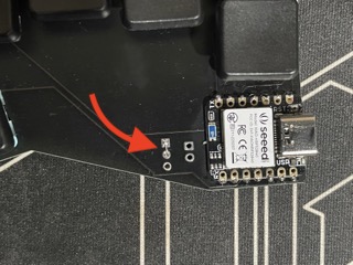
For the left hand side, need to jumper the bottom two holes as shown below:
Kiai is an open-source printed circuit board by makgyber, from the makgyber/kiai-split repository on GitHub. It is a 2-layer board of 101.4 × 90.9 mm with 20 parts on 23 nets, routed with 172 tracks and 0 vias.
Its parts include 17 switches and 1 IC. It belongs with the nRF52 and nRF5x boards of this library.
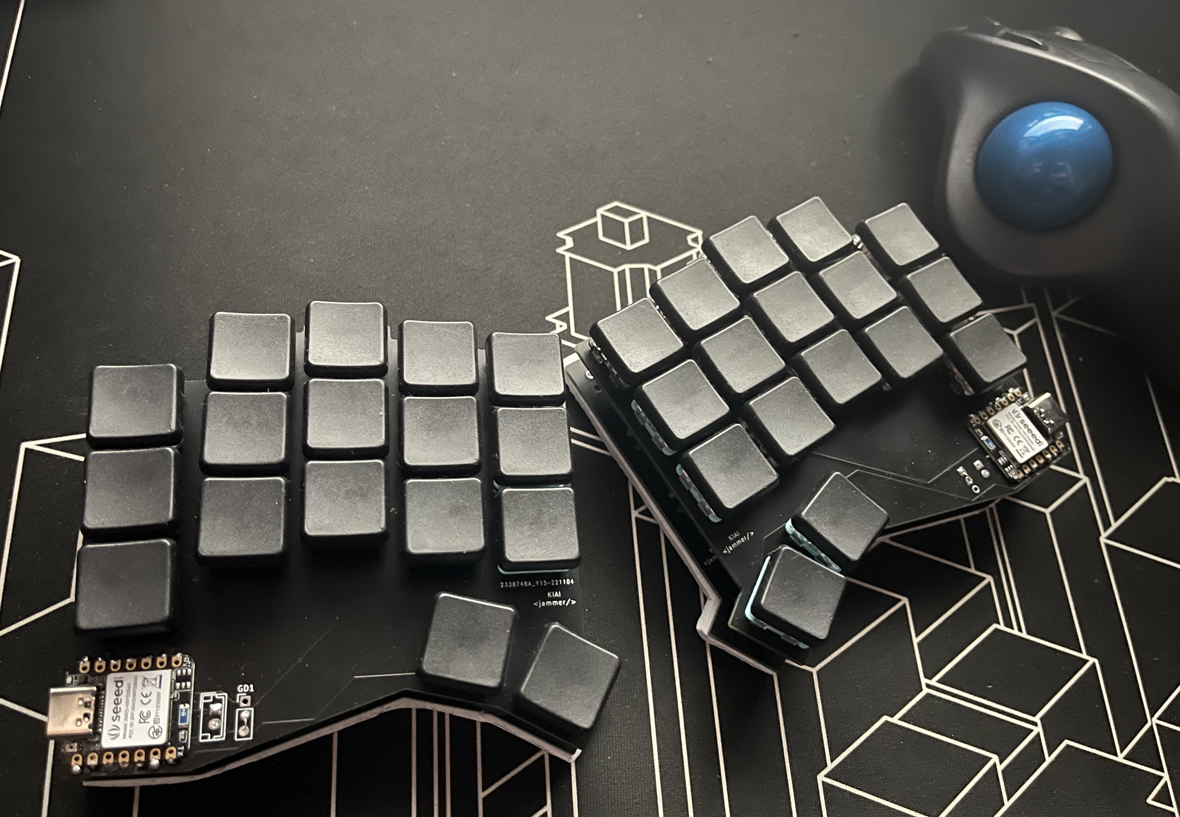
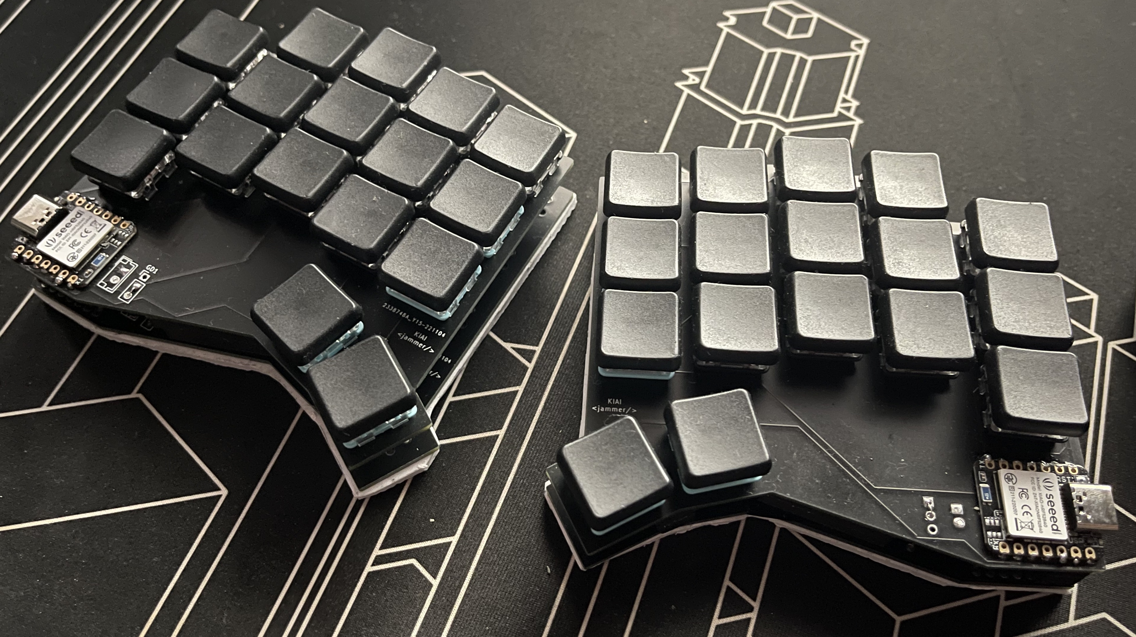
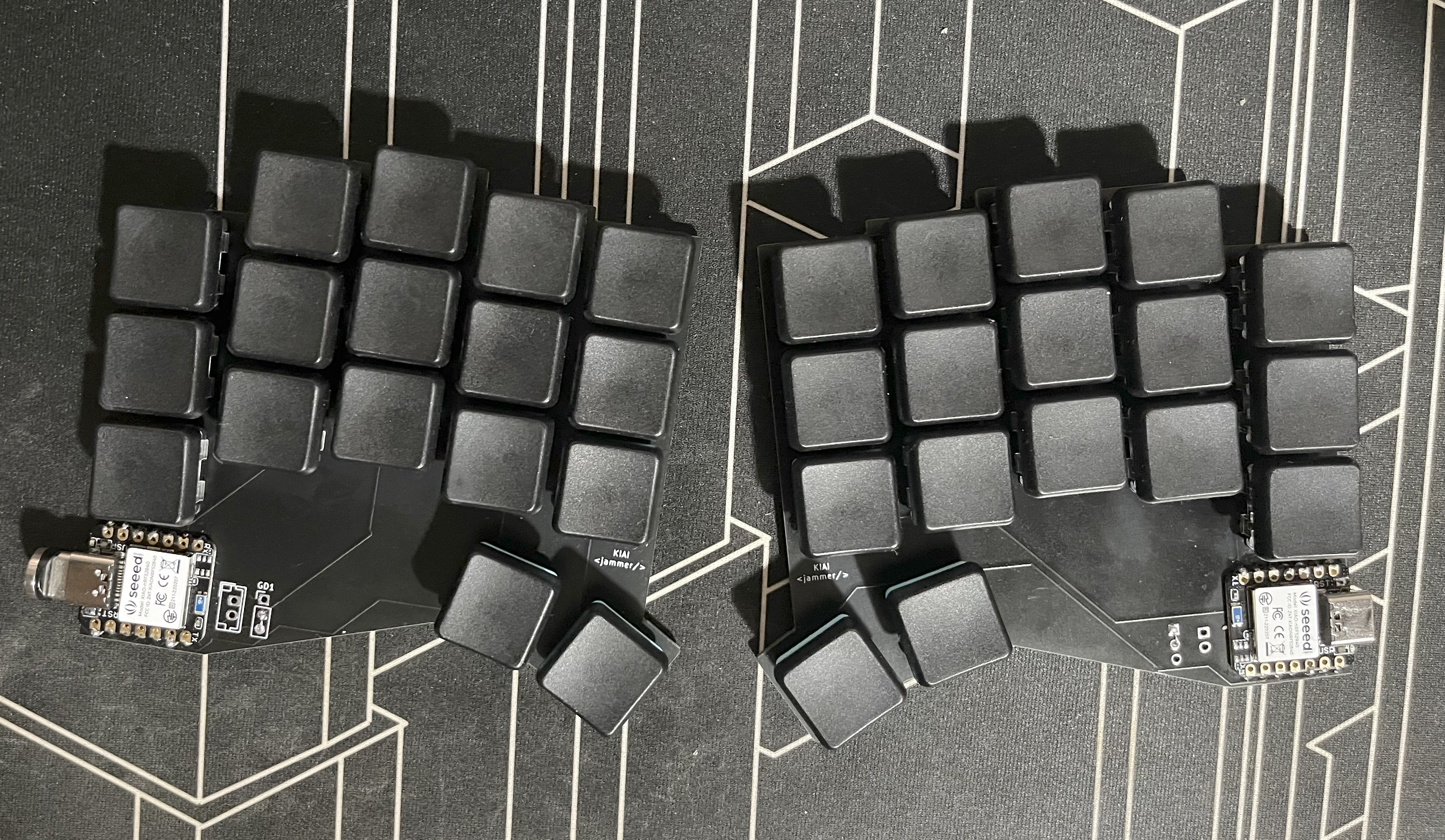
Because I wanted to have the xiao modules both facing up so the built-in reset button on the xiao is readily accessible, there are a couple of things that may be different from how other boards are normally set up.
For the left hand side, need to jumper the bottom two holes as shown below:
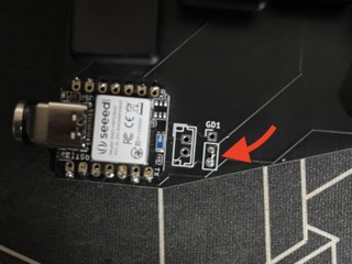
The right side will also need the jumper but on the upper two holes instead:
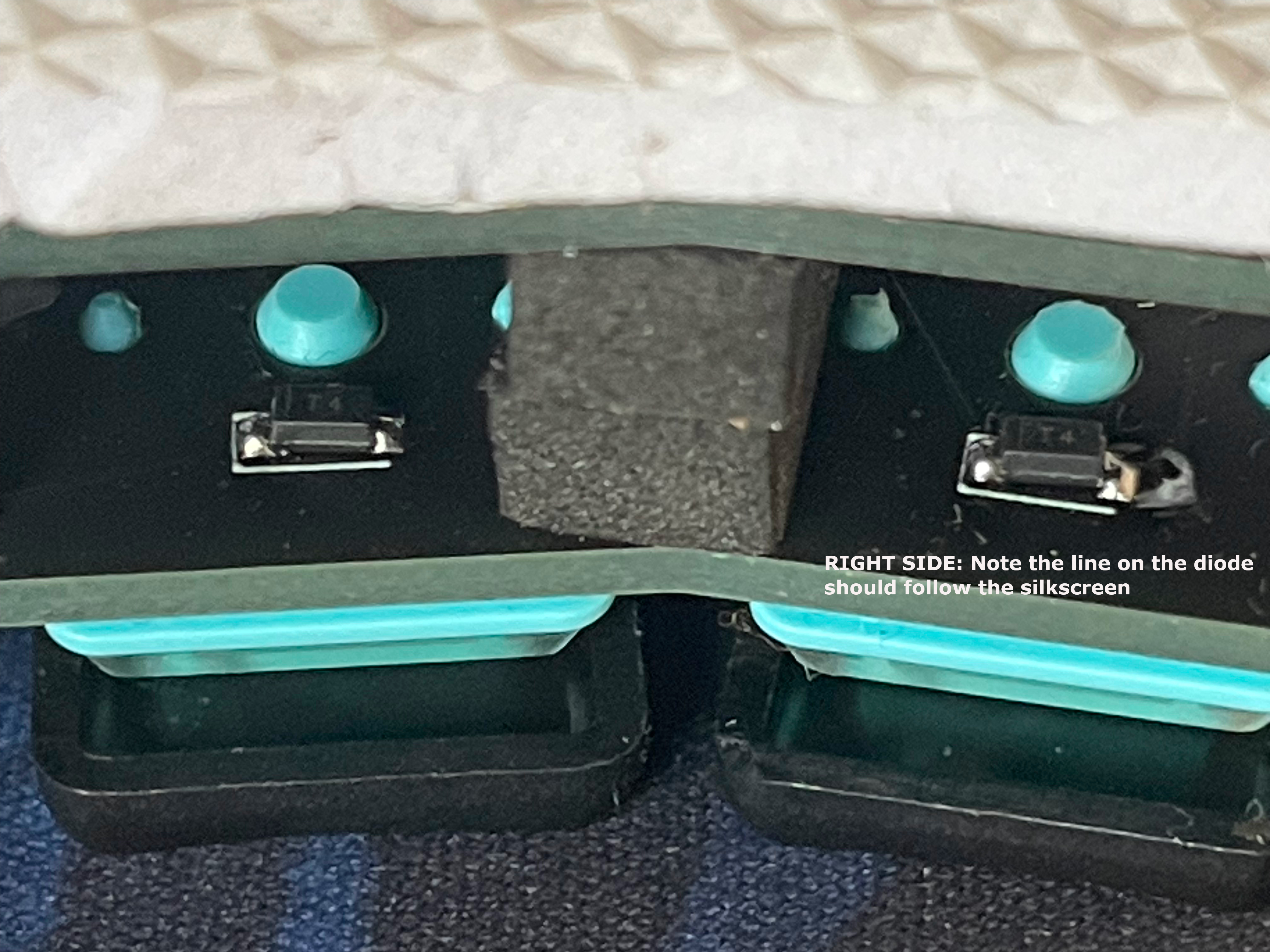
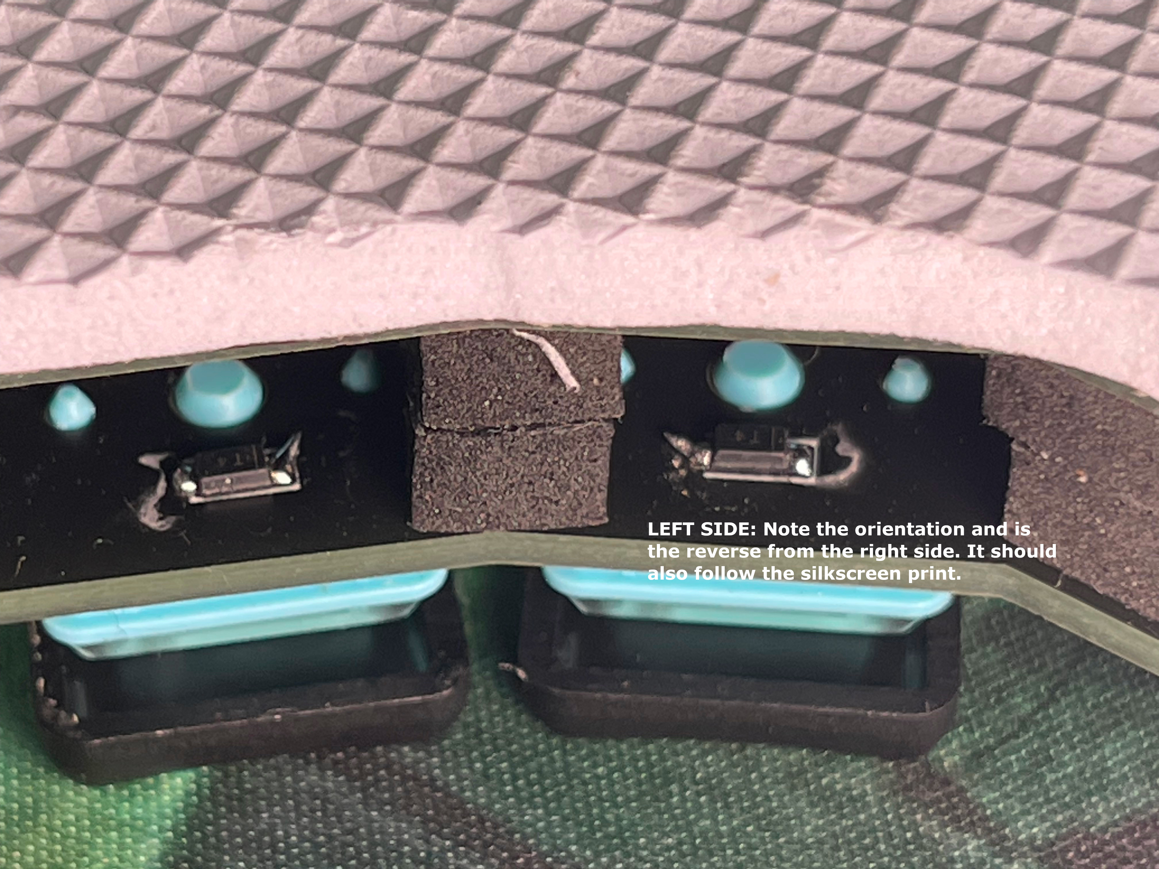
The diodes should mirror the orientation on the opposite board.
For convenience, the compiled uf2 files are in the bin folder.
left.uf2 -> for the left side
right.uf2 -> for the right side
reset.uf2 -> can be flashed to both boards to reset. I found this useful when the slave side is not pairing with the master side.
left.uf2 onto that folder. It will automatically eject after.right.uf2 file.install ZMK following this guide: ZMK Basic Setup
in your {zmk-dir}/app/board/shields directory, create a folder named kiai
copy the files in the zmk folder in this repo into your new kiai directory
compile the hex file for your left board using
west build -p -b seeeduino_xiai_ble -d build/kiai/left -- -DSHIELD=kiai_left
this will create a zmk.uf2 file in {zmk-dir}/app/build/kiai/left/zephyr
use this file to flash the left-side board
compile the hex file for your right-side board using
west build -p -b seeeduino_xiai_ble -d build/kiai/right -- -DSHIELD=kiai_right
this will create a zmk.uf2 file in {zmk-dir}/app/build/kiai/right/zephyr
use this file to flash the right-side board
| Qty | Value | Footprint | References |
|---|---|---|---|
| 17 | diode-choc | kleeb-pg1350:pg1350-DR | K1, K2, K3, K4, K5, K6, K7, K8, K10, K11, K12, K13, K14, K15, K16, K17 +1 |
| 1 | Battery | Connector_JST:JST_EH_B2B-EH-A_1x02_P2.50mm_Vertical | BT1 |
| 1 | GDT_3Pin | Connector_PinHeader_2.54mm:PinHeader_1x03_P2.54mm_Vertical | GD1 |
| 1 | xiao-ble | kleeb-mcu:xiao-ble-tht | U1 |
It measures 101.4 × 90.9 mm and has 2 copper layers, 1.6 mm thick.
20 parts. The full list of its parts is on this page, with links to each part's symbol and footprint where PCBKit's library has them.
From the makgyber/kiai-split repository on GitHub, at the commit this page was made from: the board is kicad/kiai.kicad_pcb and its schematic kicad/kiai.kicad_sch. PCBKit opens the board in the browser, with nothing to install.
Its repository states no licence, so its author keeps all rights: ask makgyber before reusing the design.


atopile/atopile
Design circuit boards with code! ✨ Get software-like design reuse 🚀, validation, version control and collaboration in hardware; starting with electronics ⚡️

davidphilipbarr/Sweep
Sweep - a small promicro based keyboard inspired by the Ferris.

rusefi/rusefi
rusefi - GPL internal combustion engine control unit

hoglet67/RGBtoHDMI
Bare-metal Raspberry Pi project that provides pixel-perfect sampling of Retro Computer RGB/YUV video and conversion to HDMI

hackclub/OnBoard
💡 Join 1,000 teenagers and make your first PCB with a $100 grant!

FreeYourStream/freedeck-hardware
all the stuff you need to build your own FreeDeck