
2 layers25.4 × 25.4 mm
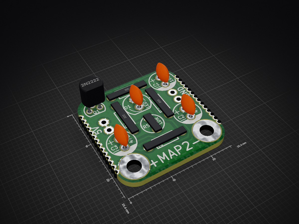
learn to solder kit, through hole, interactive art
Map2 is an open-source printed circuit board by MakersAsylumIndia, from the MakersAsylumIndia/MAP2 repository on GitHub. It is a 2-layer board of 25.4 × 25.4 mm with 45 parts on 7 nets, routed with 123 tracks and 0 vias.
Its parts include 7 connectors, 5 resistors, 3 capacitors, 1 diode and 1 transistor.
Maker's Asylum Project #2
"learn to solder kit, through hole, interactive art"
DISCUSSION FORUM : http://discuss.makersasylum.com/t/map2-learn-to-solder-kit-interactive-art-wall/68
Through Hole Version


SMD + Through Hole Version (MAP2_smd)


| Qty | Value | Footprint | References |
|---|---|---|---|
| 2 | 47uF | map2:Capacitor5x6RM2.5 | C2, C3 |
| 2 | 5V | map2:Pin_Header_Straight_1x01 | P1, P2 |
| 2 | GND | map2:Pin_Header_Straight_1x01 | P4, P5 |
| 2 | MTG | map2:MTG_3mm | P7, P8 |
| 1 | 100uF | map2:Capacitor5x6RM2.5 | C1 |
| 1 | 1M | map2:Resistor_Horizontal_RM8mm | R2 |
| 1 | 270E | map2:Resistor_Horizontal_RM8mm | R4 |
| 1 | 2N2222 | map2:TO-92_Molded_Narrow | Q1 |
| 1 | 2k2 | map2:Resistor_Horizontal_RM8mm | R1 |
| 1 | 3k3 | map2:Resistor_Horizontal_RM8mm | R3 |
| 1 | LDR | map2:R_photo | R5 |
| 1 | LED | map2:LED-5MM | D1 |
| 1 | LOGO | map2:MA_logo | P9 |
The 17 most common of 45 parts.
It measures 25.4 × 25.4 mm and has 2 copper layers, 1.6 mm thick.
45 parts. The full list of its parts is on this page, with links to each part's symbol and footprint where PCBKit's library has them.
From the MakersAsylumIndia/MAP2 repository on GitHub, at the commit this page was made from: the board is kicad/map2.kicad_pcb. PCBKit opens the board in the browser, with nothing to install.
Its repository states no licence, so its author keeps all rights: ask MakersAsylumIndia before reusing the design.


imchipwood/dumbpad
Simple 4x4 numpad with rotary encoder. Powered by QMK via ATmega32u4 Pro Micro


makeo/PicoLoader
A cheap and easy to install modchip for the Nintendo GameCube!


peterkrull/quad
Firmware, hardware and documentation for my autonomous quad copter project

tebl/RC6502-Apple-1-Replica
An expandable SBC-version of the Apple 1 computer, easy to get started with and lot of cool stuff that can be added to it!
