2 layers27.7 × 30 mm

 mackieks/fujiflex40
GCVideo DVI flex PCB for Nintendo Wii
Fujiflex is an open-source printed circuit board by mackieks, from the mackieks/fujiflex repository on GitHub. It is a 2-layer board of 27.7 × 43.7 mm with 33 parts on 79 nets, routed with 620 tracks and 218 vias.
It is built around the XC3S200A-4VQG100C and AT25SF041B-MAHD-T. Its parts include 11 capacitors, 7 resistors, 3 ICs, 1 diode and 1 connector. It belongs with the retro computing and games boards and the FPGA and CPLD boards of this library.


OSHW GCVideo DVI flex for Nintendo Wii. Tested and working! Solderpad Hardware License v2.1

Special thanks to loopj for testing the FPC and writing the assembly+install documentation!

I maintain a Mouser project with most of the BOM. You still need to source the FPGA from elsewhere. I suggest either LCSC, AliExpress, or Taobao.
The total BOM cost for fujiflex is around 10USD. If you're paying more than $5 per FPGA, you are being ripped off!
Use the provided ibom.html to guide part placement.
Note: If you intend to program the SPI flash in-system, do not place R6. You will need to place it after programming is complete.
Once assembled, you'll need to flash the GCVideo bitstream. The cheap 'n' easy approach is to program in-system using a SPI flash programmer (EZP20xx, CH341A-based, RPi Pico) soldered to the testpads on fujiflex.
gcvideo-dvi-shuriken-v3-wii-3.1-spirom-complete.bin) to the SPI flash (see below)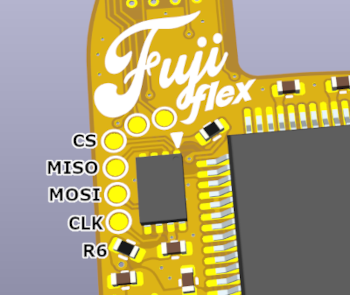
If you are using an EZP20xx programmer, you can flash the bitstream using the Windows software for these devices.
flashrom)For other programmers, flashrom is an open source command line tool for programming flash chips which supports tons of devices, including the inexpensive CH341A-based boards.
First expand the GCVideo bitstream to match the size of the SPI flash chip:
fallocate -l 512k gcvideo-dvi-shuriken-v3-wii-3.1-spirom-complete.binThen flash the bitstream, for example with a CH341A programmer:
flashrom --programmer ch341a_spi -w gcvideo-dvi-shuriken-v3-wii-3.1-spirom-complete.binYou can also use a DFN8 2x3mm socket to program the SPI flash before soldering it to the board. Type 1, Type 2
fujiflex is soldered directly to the digital A/V vias on a 4-layer Wii motherboard.
Installation Photo:

Solderpad Hardware License v2.1
| Qty | Value | Footprint | References |
|---|---|---|---|
| 9 | 0.1uF | Capacitor_SMD:C_0402_1005Metric | C3, C4, C5, C6, C7, C8, C9, C10, C12 |
| 4 | TestPoint | SamacSys_Parts:TestPoint_Pad_D0.75mm | TP6, TP7, TP8, TP9 |
| 3 | TestPoint | TestPoint:TestPoint_Pad_D1.5mm | TP1, TP2, TP3 |
| 2 | 10k | Resistor_SMD:R_0402_1005Metric | R1, R2 |
| 2 | 1uF | Capacitor_SMD:C_0402_1005Metric | C1, C2 |
| 2 | 4.7k | Resistor_SMD:R_0402_1005Metric | R4, R7 |
| 2 | TestPoint | TestPoint:TestPoint_Pad_D1.0mm | TP4, TP5 |
| 1 | 0 | Resistor_SMD:R_0402_1005Metric | R6 |
| 1 | 100K | Resistor_SMD:R_0402_1005Metric | R5 |
| 1 | 330 | Resistor_SMD:R_0402_1005Metric | R3 |
| 1 | 505278-1933 | SamacSys_Parts:5052781933 | J1 |
| 1 | AP2127N-1.2 | Package_TO_SOT_SMD:SOT-23 | U3 |
| 1 | AT25SF041B-MAHD-T | SamacSys_Parts:SON50P300X200X60-9N-D | U2 |
| 1 | BAT54XV2T1G | Diode_SMD:D_SOD-523 | D1 |
| 1 | SolderJumper_2_Open | Jumper:SolderJumper-2_P1.3mm_Open_RoundedPad1.0x1.5mm | JP1 |
| 1 | XC3S200A-4VQG100C | SamacSys_Parts:QFP50P1600X1600X120-100N | U1 |


VoxelTek/ComboFlex
A combination of assistive flexible PCBs for Wii modding and portabilising.

hoglet67/RGBtoHDMI
Bare-metal Raspberry Pi project that provides pixel-perfect sampling of Retro Computer RGB/YUV video and conversion to HDMI

mntmn/amiga2000-gfxcard
MNT VA2000, an Open Source Amiga 2/3/4000 Graphics Card (Zorro II/III), written in Verilog

hackclub/OnBoard
💡 Join 1,000 teenagers and make your first PCB with a $100 grant!

Arrow-air/project-quiver
Project Quiver documentation, designs, and project artifacts.

ozel/DIY_particle_detector
A mobile low-cost spectrometer for measuring radioactivity and the energy of ionising radiation like alpha particles and electrons

BlueAndi/Pixelix
Full RGB LED matrix, based on an ESP32 and WS2812B LEDs or emulated LEDs on TFT.

jrsteensen/OpenHornet
OpenHornet 1:1 F/A-18C Simulator Repository
It measures 27.7 × 43.7 mm and has 2 copper layers, 0.11 mm thick.
33 parts, built around the XC3S200A-4VQG100C and AT25SF041B-MAHD-T. The full list of its parts is on this page, with links to each part's symbol and footprint where PCBKit's library has them.
From the mackieks/fujiflex repository on GitHub, at the commit this page was made from: the board is KiCAD/6 Layer Compatible/fujiflex.kicad_pcb and its schematic KiCAD/6 Layer Compatible/fujiflex.kicad_sch. PCBKit opens the board in the browser, with nothing to install.
Its repository states no licence, so its author keeps all rights: ask mackieks before reusing the design.