4 layers65 × 100 mm

 m0tei/StrainGauge
A very small analog amplifier board for a full-bridge strain gauge on a carbon rod. It powers the bridge, amplifies the tiny bridge signal by about 151, filters it, and sends one analog voltage to an ADC.
StrainGauge is an open-source printed circuit board by m0tei, from the m0tei/StrainGauge repository on GitHub. It is a 2-layer board of 18.3 × 5 mm with 22 parts on 15 nets, routed with 103 tracks and 15 vias.
It is built around the MCP6N16-100E/MS, OPA388QDBVRQ1 and TPS7A2033PDBVR-TP, with the TPD1E10B06QDPYRQ1, RG1005N-104-W-T1 and GCM188R71C334KA37D among its other parts. Its parts include 7 capacitors, 5 resistors, 3 ICs, 2 diodes and 2 connectors.


A very small analog amplifier board for a full-bridge strain gauge on a carbon rod. It powers the bridge, amplifies the tiny bridge signal by about 151, filters it, and sends one analog voltage to an ADC.
| Board size | 18.35 × 5.0 mm, 0.8 mm thick, 2 layers |
| Supply | 5 V in, 3.3 V on board |
| Output | Analog, 0.825 V at zero strain |
| Sensitivity | About 0.649 mV/µε at the output |
| Usable range | About 3730 µε compression, 1190 µε extension |
| Bandwidth | About 480 Hz |
| Bridge | 350 Ω full bridge, 3.3 V excitation |
| Design tool | KiCad 10 |
Sensitivity and range assume a gauge factor of 2 and a Poisson ratio of 0.3. Replace these with your gauge and rod values when calibrating.
Status: this is a design that passes KiCad's electrical and layout checks. This repository has no test results from a built board. See Before ordering.
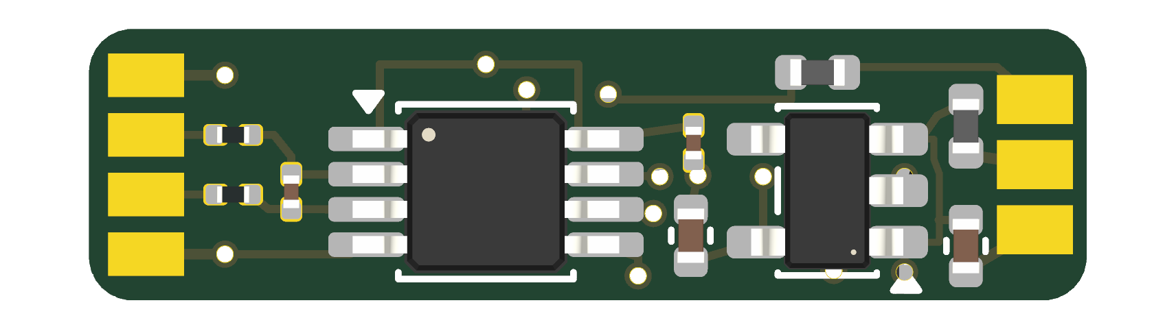
Top side: amplifier U2, regulator U1, input filter, and ferrites. The gauge pads J2 are on the left and the cable pads J1 are on the right.
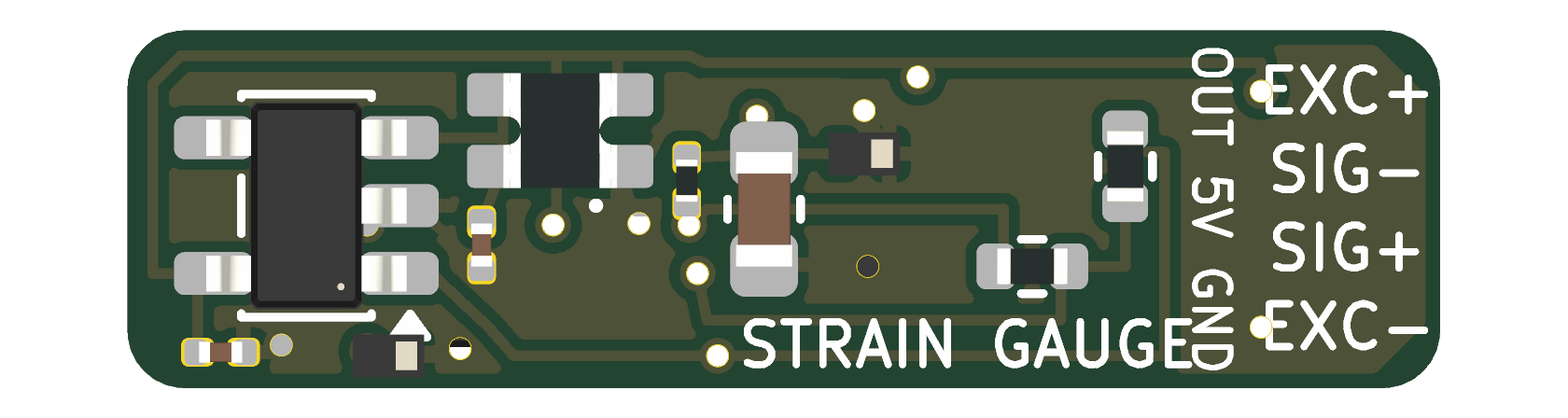
Bottom side: VREF buffer U3, VREF divider RN1, gain resistors R1 and R2, output filter R4 and C5, and ESD diodes D1 and D2. This view is flipped, so J2 is on the right.
flowchart LR
    A[5 V from J1] --> B[FB1 and D1]
    B --> C[U1 3.3 V regulator]
    C --> D[Strain gauge bridge]
    C --> E[RN1 and U3 make 0.825 V VREF]
    D --> F[Input filter]
    F --> G[U2 amplifier, gain 151]
    E --> G
    G --> H[R4 and C5 output filter]
    H --> I[FB2 and D2]
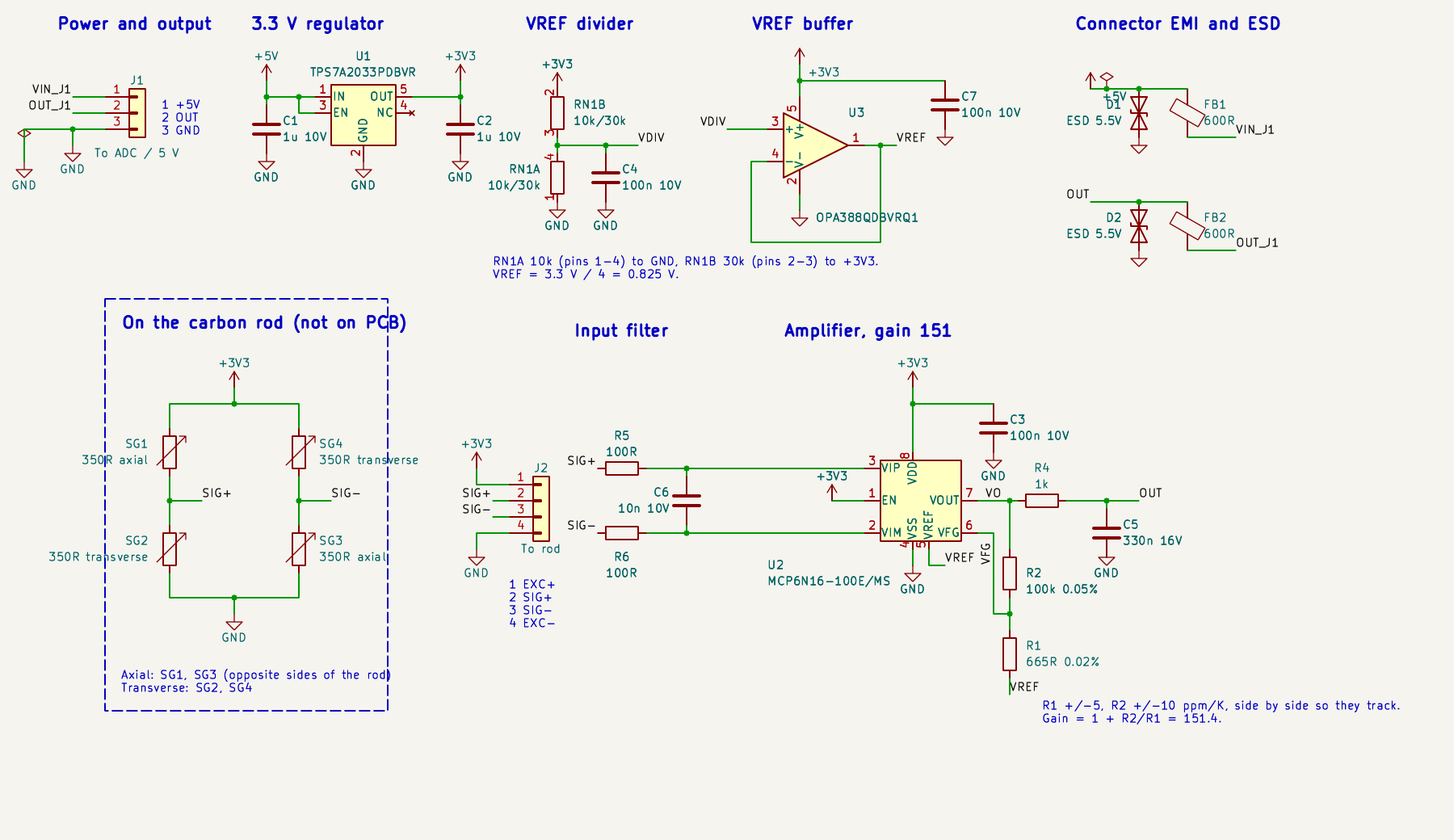
I --> J[OUT on J1]Four 350 Ω gauges are bonded to the rod. SG1 and SG3 are axial and sit on opposite sides of the rod. SG2 and SG4 are transverse.
Bending affects the two axial gauges in opposite directions, so it largely cancels. Pure tension or compression adds up. With a 3.3 V supply, the bridge gives about 4.3 µV for each microstrain.
The 5 V input passes through ferrite FB1, which keeps high-frequency noise out of the regulator. D1 clamps spikes from the cable.
U1 (TPS7A2033) makes the 3.3 V rail. It powers the amplifier and the bridge, and it is also the source for VREF. The bridge draws about 9.4 mA.
RN1 is a 10k/30k pair that divides 3.3 V by four, and U3 buffers it to make a low-impedance 0.825 V VREF. This sets the amplifier's zero point. It sits low because the expected load is lopsided: 3000 µε compression and 300 µε extension. Compression drives the output up, and extension drives it down.
R5, R6, and C6 form a differential low-pass filter with a corner of about 29 kHz, including the bridge resistance. It reduces high-frequency interference picked up on the gauge wires.
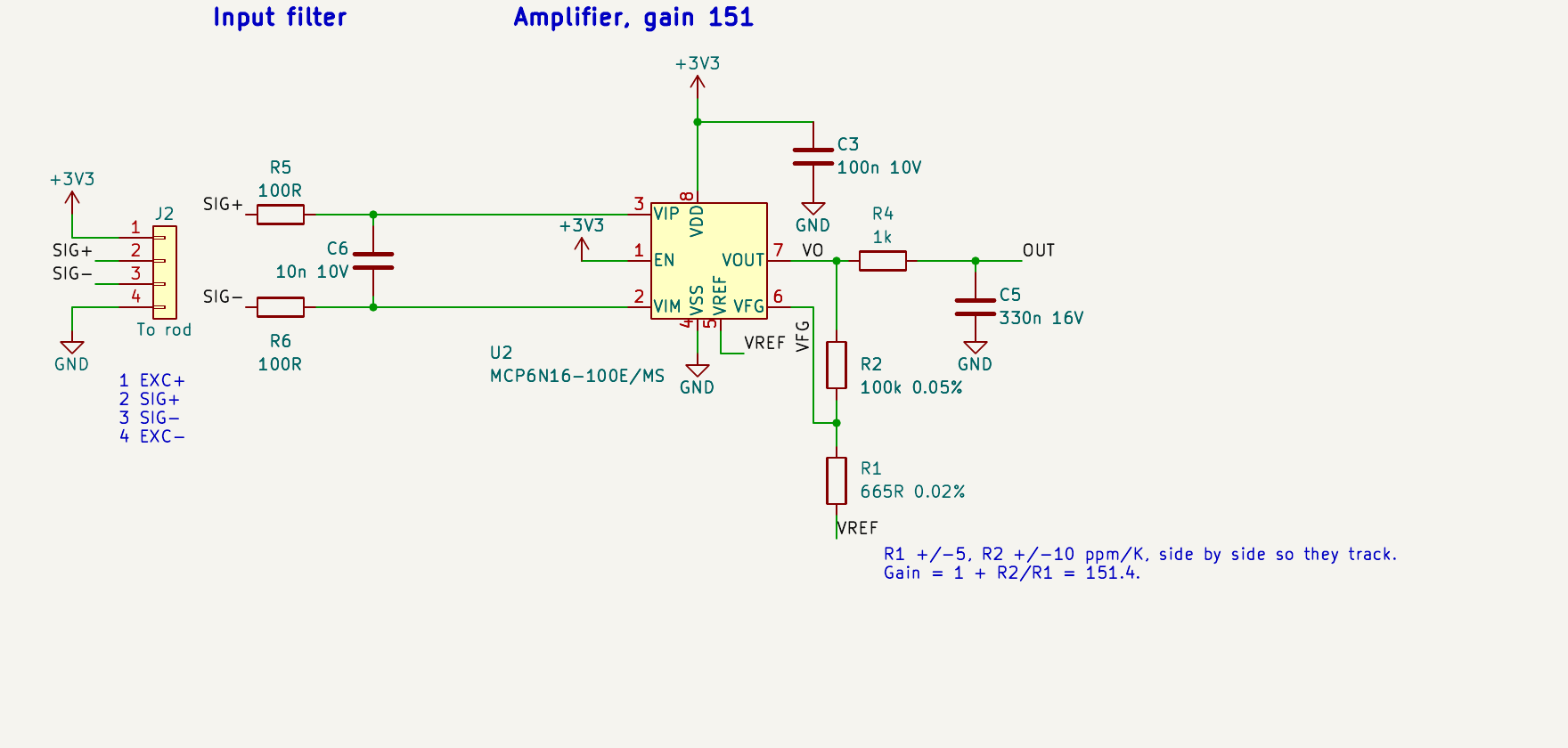
U2 (MCP6N16-100) is a zero-drift instrumentation amplifier. Zero drift means it constantly corrects its own offset, which suits slow, tiny signals like this one.
Two external resistors set the gain:
Gain = 1 + R2 / R1 = 1 + 100k / 665 = 151.4The gain depends on the ratio of R2 to R1, not their absolute values. R1 is rated ±5 ppm/K and R2 ±10 ppm/K. They come from the same Susumu RG1005 range and sit next to each other, so their ratio stays stable as temperature changes.
The output is:
VOUT = VREF + Gain × (SIG+ − SIG−)R4 and C5 form a low-pass filter at about 480 Hz. This removes noise above the signal band and isolates the amplifier from the cable. FB2 and D2 add high-frequency blocking and ESD protection at the output.
Use the labels printed on the board, because the J2 pad order is not the same as its pin numbers.
J2, gauge bridge (top to bottom on the board):
| Label | Pin | Connects to |
|---|---|---|
| EXC+ | 1 | Bridge top, 3.3 V |
| SIG− | 3 | Junction of SG4 and SG3 |
| SIG+ | 2 | Junction of SG1 and SG2 |
| EXC− | 4 | Bridge bottom, GND |
J1, cable to the ADC (top to bottom on the board):
| Signal | Pin | Notes |
|---|---|---|
| OUT | 2 | Analog output |
| +5V | 1 | Power input |
| GND | 3 | Ground |
The OUT 5V GND silk label is on the back of the board near J2, not beside J1. Follow the table above when wiring J1.
Convert the voltage to strain with the line below, where compression is positive:
strain (µε) = (VOUT − 0.825 V) / 0.000649 V per µεTreat this as a starting point. For real measurements, calibrate the board on the rod with known loads, and measure the zero point at no load.
Both the zero point and the sensitivity follow the 3.3 V rail, and the ADC cannot see that rail through J1. See the first item below.
The full list with manufacturers, ratings, and sources is in StrainGauge_BOM.csv.
| Ref | Part | Purpose |
|---|---|---|
| U1 | TI TPS7A2033PDBVR | 3.3 V regulator |
| U2 | Microchip MCP6N16-100E/MS | Zero-drift instrumentation amplifier |
| U3 | TI OPA388QDBVRQ1 | VREF buffer |
| R1 | Susumu RG1005V-6650-P-T1, 665 Ω | Gain setting |
| R2 | Susumu RG1005N-104-W-T1, 100 kΩ | Gain setting |
| RN1 | Vishay ACASN1002U3002P1AT, 10k/30k | VREF divider |
| R4 | 1 kΩ | Output filter |
| R5, R6 | 100 Ω | Input filter |
| C1, C2 | 1 µF | Regulator input and output |
| C3, C4, C7 | 100 nF | Decoupling and VREF filtering |
| C5 | 330 nF | Output filter |
| C6 | 10 nF | Input filter |
| FB1, FB2 | Murata BLM15PX601SH1D | Connector EMI filtering |
| D1, D2 | TI TPD1E10B06QDPYRQ1 | ESD protection |
| File | Contents |
|---|---|
StrainGauge.kicad_pro | KiCad project, open this first |
StrainGauge.kicad_sch | Schematic |
StrainGauge.kicad_pcb | PCB layout |
StrainGauge.kicad_sym | Project symbols |
StrainGauge.pretty/ | Project footprints |
StrainGauge_BOM.csv | Bill of materials |
StrainGauge_top.png, StrainGauge_bottom.png | Board renders |
docs/ | Schematic images used in this README |
| Qty | Value | Footprint | References |
|---|---|---|---|
| 3 | 100n 10V | Capacitor_SMD:C_0201_0603Metric | C3, C4, C7 |
| 2 | 100R | Resistor_SMD:R_0201_0603Metric | R5, R6 |
| 2 | 1u 10V | Capacitor_SMD:C_0402_1005Metric | C1, C2 |
| 2 | 600R | Inductor_SMD:L_0402_1005Metric | FB1, FB2 |
| 2 | ESD 5.5V | StrainGauge:TVS_X1SON-2_DPY | D1, D2 |
| 1 | 100k 0.05% | Resistor_SMD:R_0402_1005Metric | R2 |
| 1 | 10k/30k | StrainGauge:ACAS_0606 | RN1 |
| 1 | 10n 10V | Capacitor_SMD:C_0201_0603Metric | C6 |
| 1 | 1k | Resistor_SMD:R_0201_0603Metric | R4 |
| 1 | 330n 16V | Capacitor_SMD:C_0603_1608Metric | C5 |
| 1 | 665R 0.02% | Resistor_SMD:R_0402_1005Metric | R1 |
| 1 | MCP6N16-100E/MS | StrainGauge:Microchip_MS_MSOP-8 | U2 |
| 1 | OPA388QDBVRQ1 | StrainGauge:TI_DBV0005A_SOT-23-5 | U3 |
| 1 | TPS7A2033PDBVR | StrainGauge:TI_DBV0005A_SOT-23-5 | U1 |
| 1 | To ADC / 5 V | StrainGauge:CablePads_1x03 | J1 |
| 1 | To rod | StrainGauge:GaugePads_1x04 | J2 |


UzixLS/zxevo1010-board
10x10cm PCB variant of ZX-Evolution project for G738/G706 enclosure

UzixLS/zxuno1010-board
10x10cm PCB variant of ZX-UNO project for G738/G706 enclosure


hoeken/frothfet
Yarrboard load controller board with current sense, volt sense, fuses, and sender support.
It measures 18.3 × 5 mm and has 2 copper layers, 0.8 mm thick.
22 parts, built around the MCP6N16-100E/MS, OPA388QDBVRQ1, TPS7A2033PDBVR-TP and TPD1E10B06QDPYRQ1. The full list of its parts is on this page, with links to each part's symbol and footprint where PCBKit's library has them.
From the m0tei/StrainGauge repository on GitHub, at the commit this page was made from: the board is StrainGauge.kicad_pcb and its schematic StrainGauge.kicad_sch. PCBKit opens the board in the browser, with nothing to install.
Its repository states no licence, so its author keeps all rights: ask m0tei before reusing the design.