2 layers60 × 30 mm
Controller
google/mozc-devices
Circuit diagrams and firmware source code for Gboard DIY keyboards
11 parts3kApache-2.0

 lucy-chapar/evil-weather-machine
Carrier PCB and weather/shot-day firmware for the PrintKits Digital Sand kit
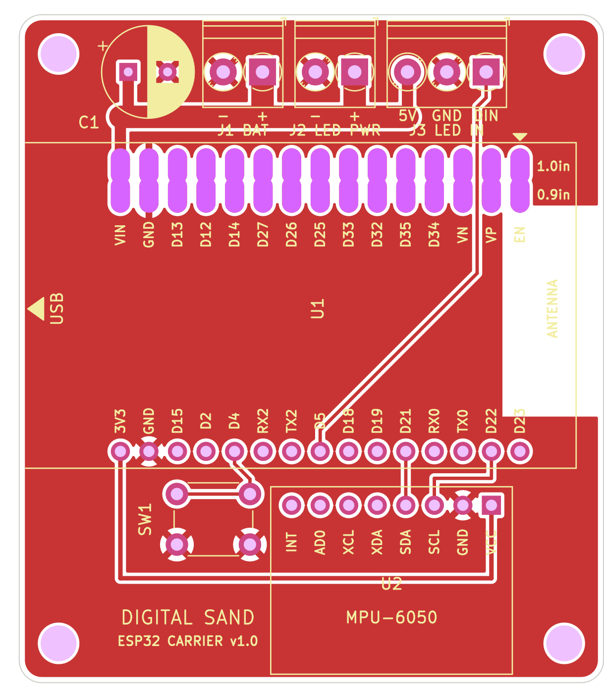
Digital sand is an open-source printed circuit board by lucy-chapar, from the lucy-chapar/evil-weather-machine repository on GitHub. It is a 2-layer board of 52 × 59.5 mm with 11 parts on 33 nets, routed with 22 tracks and 0 vias.
Its parts include 3 connectors, 2 ICs, 1 capacitor and 1 switch. It belongs with the ESP32 boards of this library.
KiCad 7 project for a two-layer board that replaces the point-to-point wiring of the PrintKits Digital Sand kit. It uses the same parts and the same connections; the board holds the parts and does the wiring.
| Path | Contents |
|---|---|
digital_sand.kicad_pro | KiCad project (open this) |
digital_sand.kicad_sch | Schematic (PDF) |
digital_sand.kicad_pcb | Board: 52 × 59.5 mm, 2 layers |
lib/ | Project symbols and footprints: ESP32 DevKit V1 30-pin, GY-521, VBAT power symbol |
docs/ | Schematic PDF and board previews |
fab/digital_sand_gerbers.zip | Gerbers and Excellon drill files |
tools/generate_kicad.py | Script that generates all of the above |
| ESP32 pin | Goes to |
|---|---|
| D5 (GPIO5) | J3 DIN → LED panel data in |
| D4 (GPIO4) | SW1 → GND |
| D21 (GPIO21) | GY-521 SDA |
| D22 (GPIO22) | GY-521 SCL |
| 3V3 | GY-521 VCC |
| VIN | VBAT rail (battery and LED panel 5 V) |
| GND | Common ground |
As in the original wiring, the 4×AA box (J1) feeds the LED panel's extra power wires (J2) directly. The ESP32 runs from the same rail through VIN.
USB arrow at the board edge,
antenna over the copper-free area marked ANTENNA.
1.0in) for
boards with 25.4 mm between header rows, and the inner row (0.9in) for 22.86 mm boards.1 pad and one 2 pad).BAT: battery red → +, black → -LED PWR: the panel's extra red wire → +, white → -LED IN: panel input red → 5V, white → GND, green → DIN+ to the square pad.tools/generate_kicad.py writes the libraries, schematic and board. It then checks the schematic netlist
against the kit wiring, fills the copper zones, runs DRC and re-exports docs/ and fab/.
Run it with KiCad 7's bundled Python, which provides pcbnew:
/Applications/KiCad/KiCad.app/Contents/Frameworks/Python.framework/Versions/Current/bin/python3 tools/generate_kicad.pyThe script overwrites the KiCad files. Once you start editing the design in KiCad itself, stop using the script.
| Qty | Value | Footprint | References |
|---|---|---|---|
| 4 | M3 | MountingHole:MountingHole_3.2mm_M3 | H1, H2, H3, H4 |
| 1 | 470uF 10V | Capacitor_THT:CP_Radial_D8.0mm_P3.50mm | C1 |
| 1 | 6mm tactile | Button_Switch_THT:SW_PUSH_6mm | SW1 |
| 1 | Battery 4xAA | TerminalBlock_Phoenix:TerminalBlock_Phoenix_PT-1,5-2-3.5-H_1x02_P3.50mm_Horizontal | J1 |
| 1 | ESP32 DevKit V1 30-pin | DigitalSand:ESP32_DevKit_V1_30pin_DualRow | U1 |
| 1 | GY-521 (MPU-6050) | DigitalSand:GY-521_MPU6050_Module | U2 |
| 1 | LED panel DIN | TerminalBlock_Phoenix:TerminalBlock_Phoenix_PT-1,5-3-3.5-H_1x03_P3.50mm_Horizontal | J3 |
| 1 | LED panel power | TerminalBlock_Phoenix:TerminalBlock_Phoenix_PT-1,5-2-3.5-H_1x02_P3.50mm_Horizontal | J2 |
google/mozc-devices
Circuit diagrams and firmware source code for Gboard DIY keyboards


FrameworkComputer/ExpansionCards
Reference designs and documentation to create Expansion Cards for the Framework Laptop

hoglet67/RGBtoHDMI
Bare-metal Raspberry Pi project that provides pixel-perfect sampling of Retro Computer RGB/YUV video and conversion to HDMI

hackclub/OnBoard
💡 Join 1,000 teenagers and make your first PCB with a $100 grant!


tardate/LittleArduinoProjects
a collection of "Little Electronic & Arduino Projects", most involving electronics or an Arduino in one way or another!

basilfx/TRADFRI-Hacking
Hacking IKEA TRÅDFRI products, such as light bulbs, window blinds and other accessories.
It measures 52 × 59.5 mm and has 2 copper layers, 1.6 mm thick.
11 parts. The full list of its parts is on this page, with links to each part's symbol and footprint where PCBKit's library has them.
From the lucy-chapar/evil-weather-machine repository on GitHub, at the commit this page was made from: the board is pcb/digital_sand.kicad_pcb and its schematic pcb/digital_sand.kicad_sch. PCBKit opens the board in the browser, with nothing to install.
Its repository states no licence, so its author keeps all rights: ask lucy-chapar before reusing the design.