
2 layers
Integracion radio mas Reg ADC
uri98/Radio-FM-and-voltage-regulator-integrated
Integrated Radio PCB Design ## Objective Design of an integrated radio circuit focusing on signal integrity and noise reduction.
19 parts

 LoZioo/DIY-Sonoff
Simple sonoff PCB built around the ESP-01 devboard.
Sonoff is an open-source printed circuit board by LoZioo, from the LoZioo/DIY-Sonoff repository on GitHub, published under the MIT licence. It is a 2-layer board of 59.2 × 42.9 mm with 27 parts on 21 nets, routed with 285 tracks and 28 vias.
It is built around the HLK-2M03. Its parts include 3 resistors, 3 connectors, 2 capacitors, 2 diodes and 2 transistors. It belongs with the microcontroller boards boards and the ESP8266 boards of this library.
Simple sonoff based on the ESP-01 devboard.
To download the needed KiCad libraries, you must cd schematics/lib and run the clone.sh script.
The STL files for the 3D enclosure could be retrived here.
C2 capacitor before soldering it because it can be too high to be mounted under the ESP-01 module.R3 resistor must be mounted if you are going to use the RST pin on the J3 header, otherwise you can place a short circuit instead.You can map the four ESP-01 GPIOs by using the solder pads JPx on the back of the PCB. For example, if you want to use the GPIO2 as an output to control the K2 relay, you can put a solder bridge on JP6 between the GPIO2 and OUT-2 labels. This feature has been introduced in this version because of the behaviour of the GPIOs during the bootloader stage and to make the circuit fully adaptable to every possible situation.
On the PCB, the IN-x pads are shorted directly to the screw terminal J2, while the OUT-x pads are shorted to the gate pin of the corresponding Qx MOSFET.
When booting an ESP8266 microcontroller, the bootloader reads the following pins to establish the boot configuration:
| GPIO15 | GPIO0 | GPIO2 | Boot mode |
|---|---|---|---|
| LOW | LOW | HIGH | Serial programming (bootloader mode) |
| LOW | HIGH | HIGH | Boot from flash |
| HIGH | ANY | ANY | Boot from SD card |
Note: On the ESP-01 dev board, the GPIO15 is not exposed and is held low by the hardware, so you can ignore the first column.
Said that, when booting the already programmed module, you must ensure that the second column configuration is selected. That's accomplished by the resistors R1 and R2 on the PCB.
| GPIO | Input | Output | Bootloader behaviour | Notes |
|---|---|---|---|---|
| GPIO0 | It must be held high during the boot phase. After, pulled up by R1. | Pulled up at boot by R1. After, it's clean. | Pulled up by R1 | Boot fails if pulled low. |
| GPIO1 | It must be held high during the boot phase. | It's the UART TX pin and when booting, the bootloader sends out debug data for ~8ms. For that reason, you should not use that pin to control a relay. | Bootloader UART debug output | Boot fails if pulled low. UART TX pin. |
| GPIO2 | It must be held high during the boot phase. After, pulled up by R2. | Pulled up at boot by R2. After, it's clean. | High at boot and pulled up by R2 | Boot fails if pulled low. |
| GPIO3 | Clean | It's the UART RX pin. It's should be high at boot but other than that, it's clean. | High at boot | UART RX pin. |
Smart plug
| \ | IN-1 | IN-2 | OUT-1 | OUT-2 |
|---|---|---|---|---|
| GPIO0 | X | |||
| GPIO1 | ||||
| GPIO2 | X | |||
| GPIO3 |
Sonoff
| \ | IN-1 | IN-2 | OUT-1 | OUT-2 |
|---|---|---|---|---|
| GPIO0 | X | |||
| GPIO1 | X | |||
| GPIO2 | X | |||
| GPIO3 | X |
To control the board, you can:
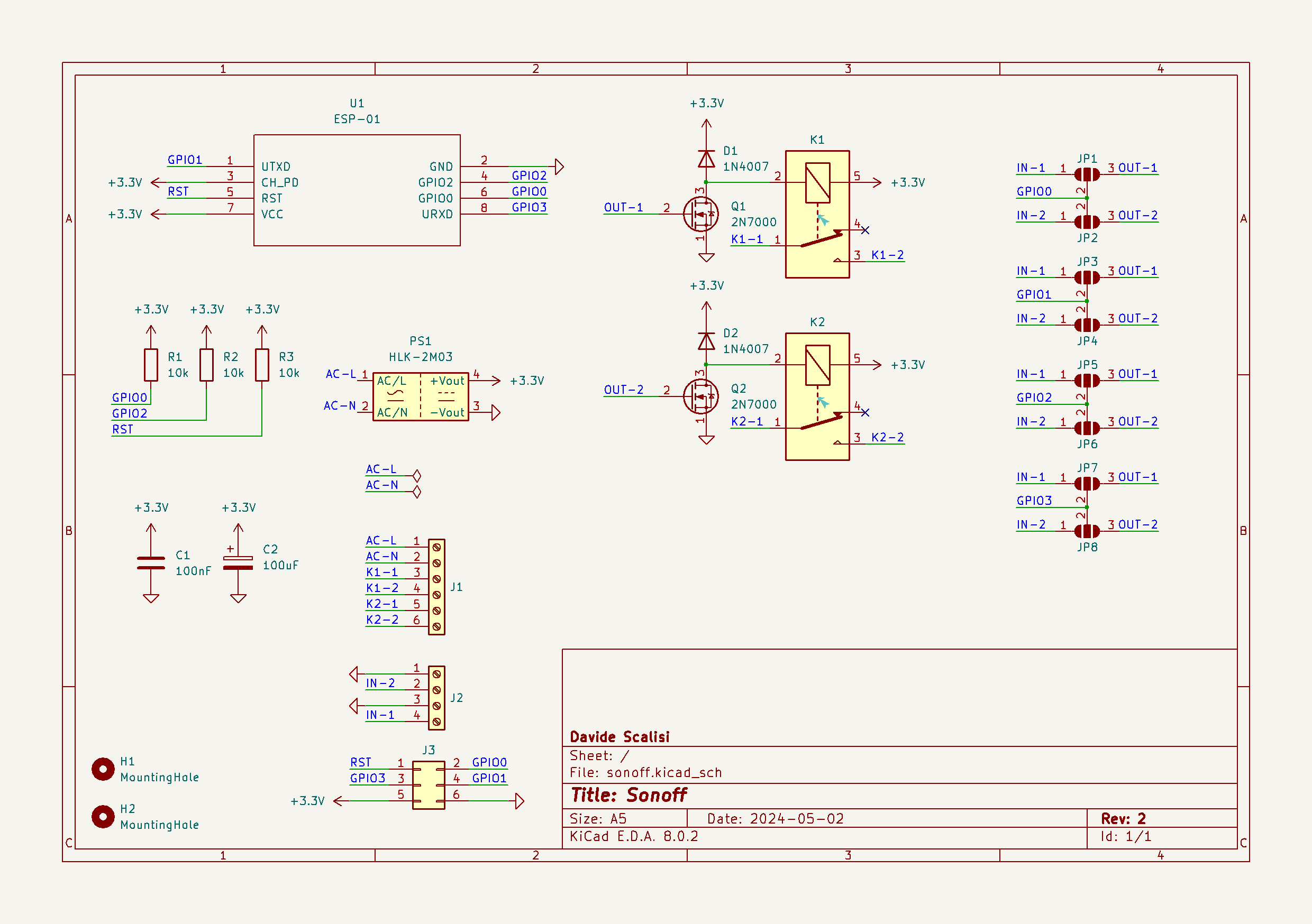
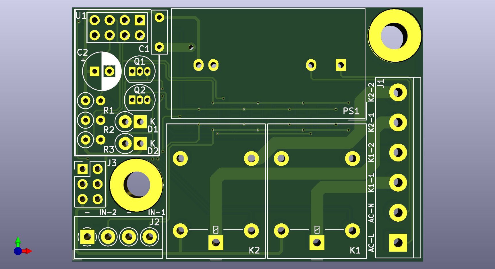
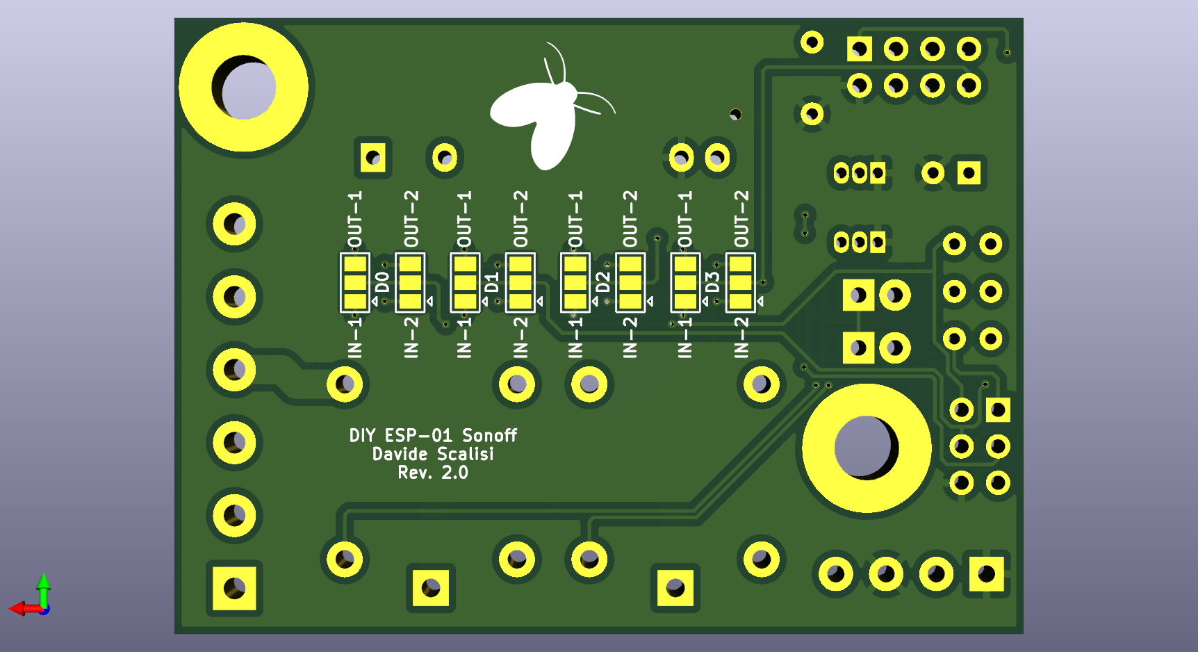
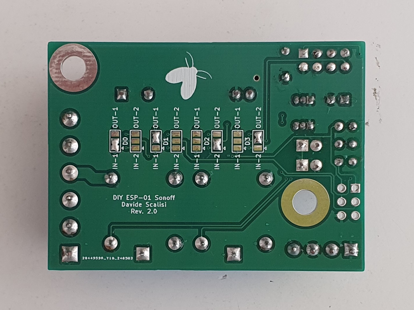
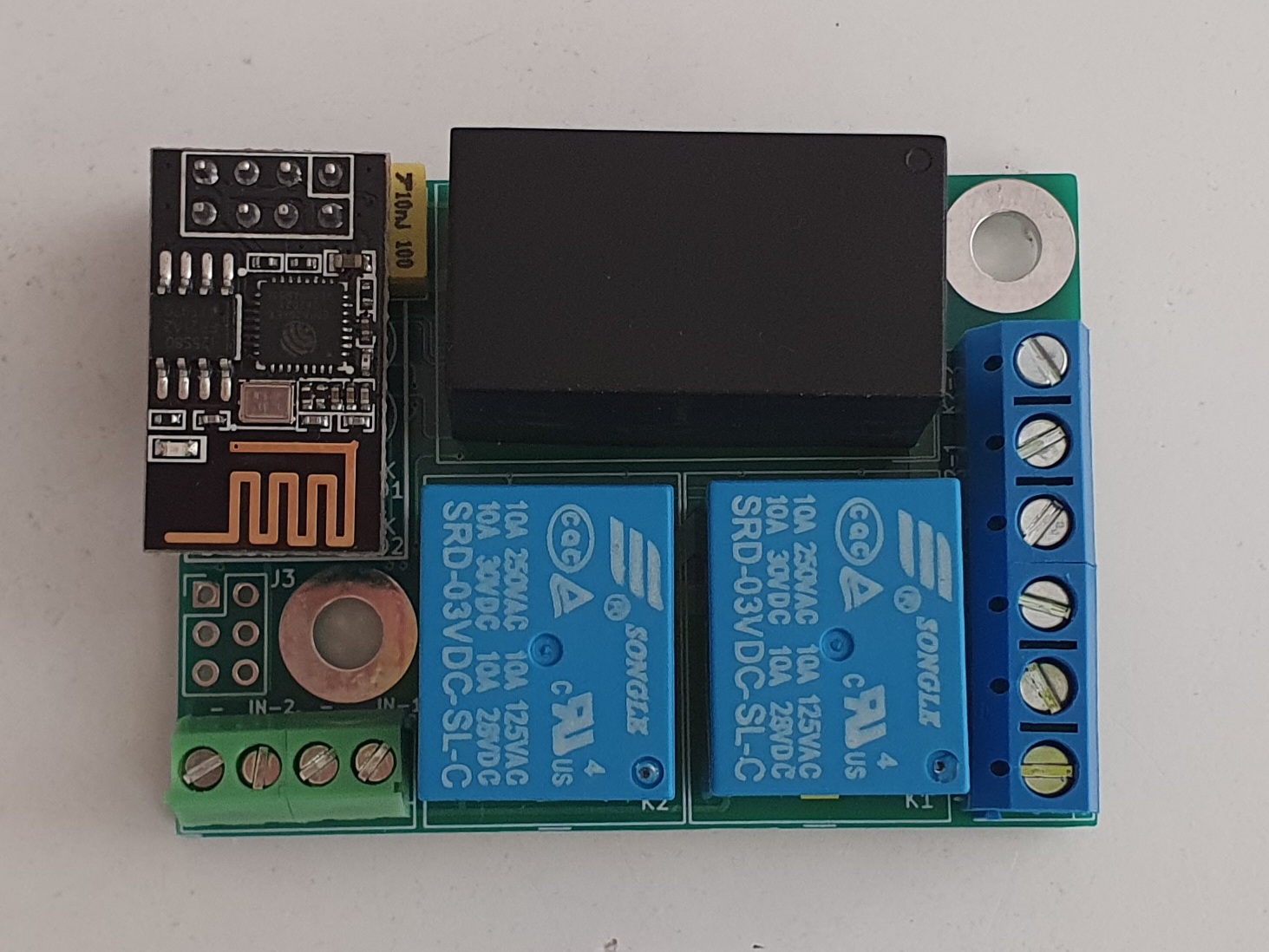
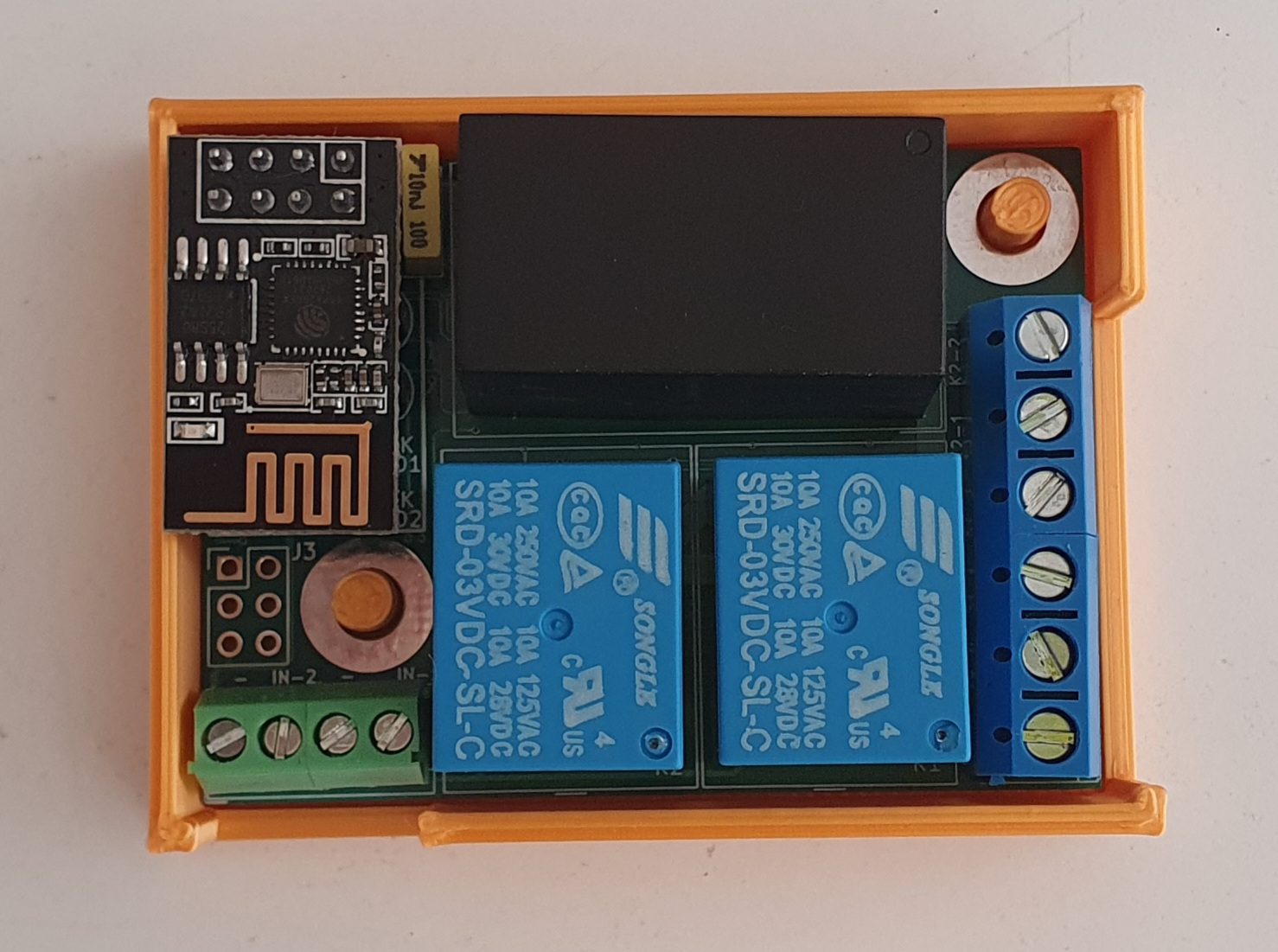
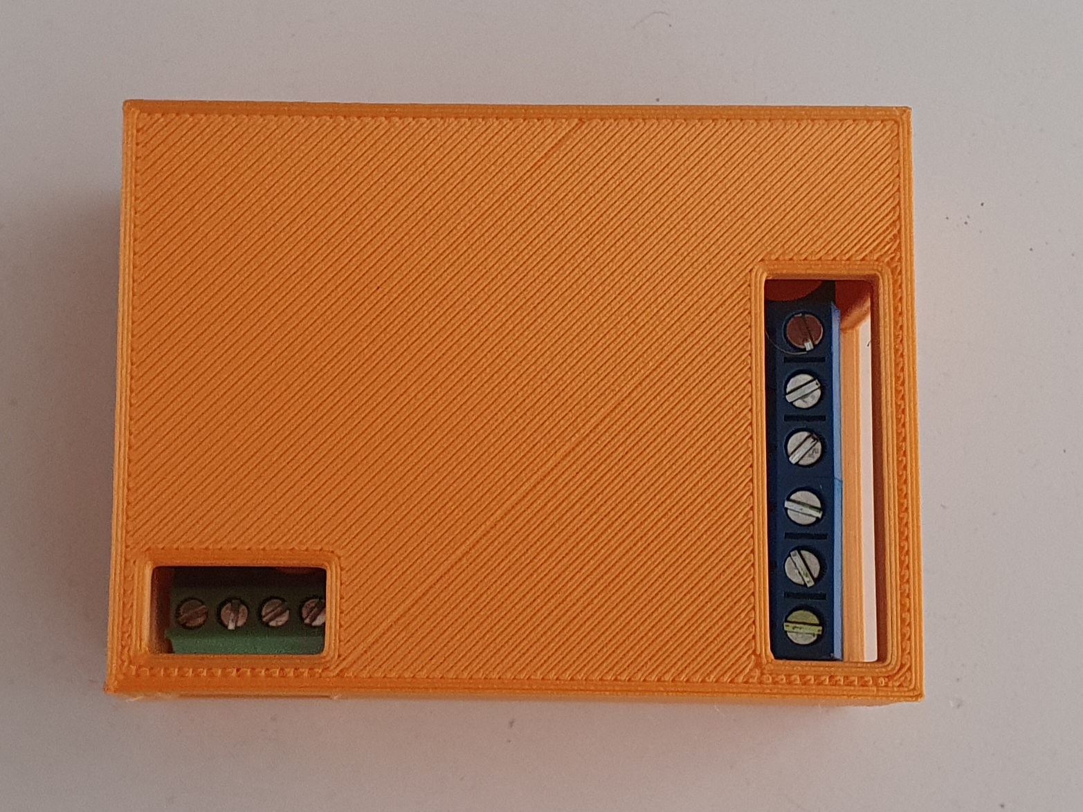
| Qty | Value | Footprint | References |
|---|---|---|---|
| 8 | SolderJumper_3_Open | Jumper:SolderJumper-3_P1.3mm_Open_Pad1.0x1.5mm | JP1, JP2, JP3, JP4, JP5, JP6, JP7, JP8 |
| 3 | 10k | Resistor_THT:R_Axial_DIN0207_L6.3mm_D2.5mm_P2.54mm_Vertical | R1, R2, R3 |
| 2 | 1N4007 | Diode_THT:D_DO-41_SOD81_P2.54mm_Vertical_KathodeUp | D1, D2 |
| 2 | 2N7000 | Package_TO_SOT_THT:TO-92_Inline | Q1, Q2 |
| 2 | MountingHole | MountingHole:MountingHole_4.5mm_Pad_TopBottom | H1, H2 |
| 2 | Relay_SPDT | Relay_THT:Relay_SPDT_Omron-G5LE-1 | K1, K2 |
| 1 | 100nF | Capacitor_THT:C_Rect_L7.2mm_W2.5mm_P5.00mm_FKS2_FKP2_MKS2_MKP2 | C1 |
| 1 | 100uF | Capacitor_THT:CP_Radial_D6.3mm_P2.50mm | C2 |
| 1 | Conn_02x03_Odd_Even | Connector_PinHeader_2.54mm:PinHeader_2x03_P2.54mm_Vertical | J3 |
| 1 | ESP-01_2x04 | ESP8266:ESP-01 | U1 |
| 1 | HLK-2M03 | Converter_ACDC:Converter_ACDC_Hi-Link_HLK-2Mxx | PS1 |
| 1 | LOGO | LOGO | G*** |
| 1 | Screw_Terminal_01x04 | TerminalBlock_4Ucon:TerminalBlock_4Ucon_1x04_P3.50mm_Horizontal | J2 |
| 1 | Screw_Terminal_01x06 | TerminalBlock:TerminalBlock_bornier-6_P5.08mm | J1 |
uri98/Radio-FM-and-voltage-regulator-integrated
Integrated Radio PCB Design ## Objective Design of an integrated radio circuit focusing on signal integrity and noise reduction.


hackclub/OnBoard
💡 Join 1,000 teenagers and make your first PCB with a $100 grant!


CRImier/MyKiCad
My KiCad boards. Can't be bothered uploading individually anymore, so here you go.

pjgpetecodes/pico-streamdeck
This project is an OBS Controller using a Raspberry Pi Pico and CircuitPython.

freeDSP/freeDSP-aurora
freeDSP ADAU1452 with 8 analog input, 8 analog outputs, S/P-DIF I/O, ADAT I/O, USB Audio Class2, WiFi, Bluetooth
It measures 59.2 × 42.9 mm and has 2 copper layers, 1.6 mm thick.
27 parts, built around the HLK-2M03. The full list of its parts is on this page, with links to each part's symbol and footprint where PCBKit's library has them.
From the LoZioo/DIY-Sonoff repository on GitHub, at the commit this page was made from: the board is schematics/sonoff.kicad_pcb and its schematic schematics/sonoff.kicad_sch. PCBKit opens the board in the browser, with nothing to install.
Its repository publishes it under the MIT licence: you may reuse it on that licence's terms (keep the author's notice, and for a copyleft licence share your changes alike).