

2 layers47.7 × 69.7 mm

 llegoff/Badges6
PCB Badges
Panel is an open-source printed circuit board by llegoff, from the llegoff/Badges repository on GitHub. It is a 2-layer board of 110 × 90 mm with 32 parts on 11 nets, routed with 162 tracks and 12 vias.
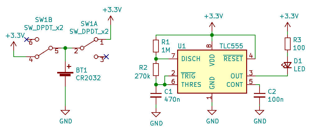
It is built around the TLC555N and CR2032. Its parts include 8 resistors, 6 diodes, 4 capacitors, 2 ICs and 2 switches.
Buy on Ebay
Calavera PCB : https://www.ebay.fr/itm/153633710557
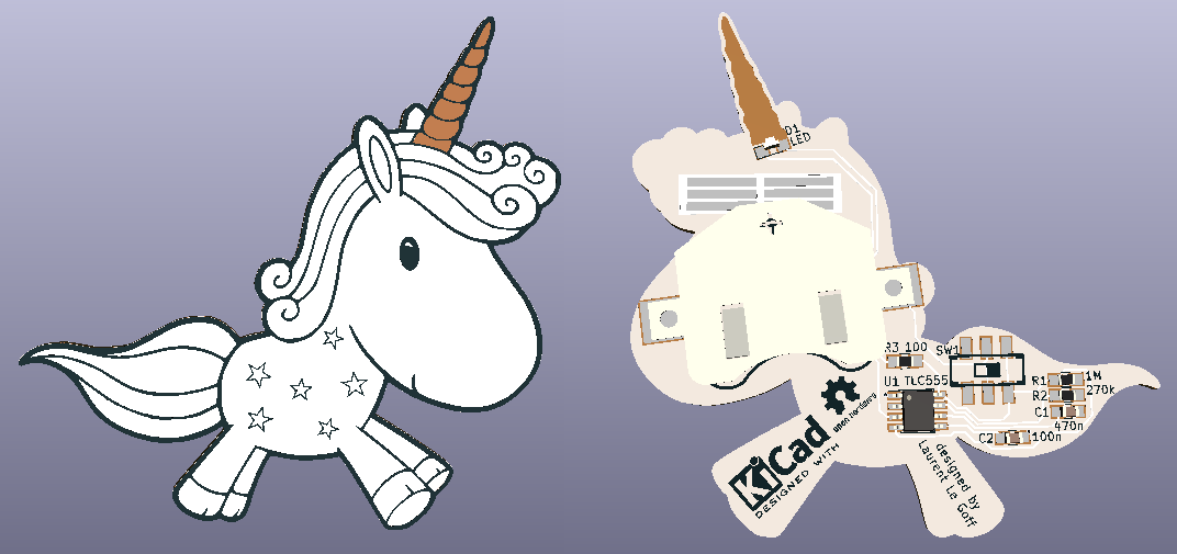
Unicorn PCB : https://www.ebay.fr/itm/153633723346
PCB Badges
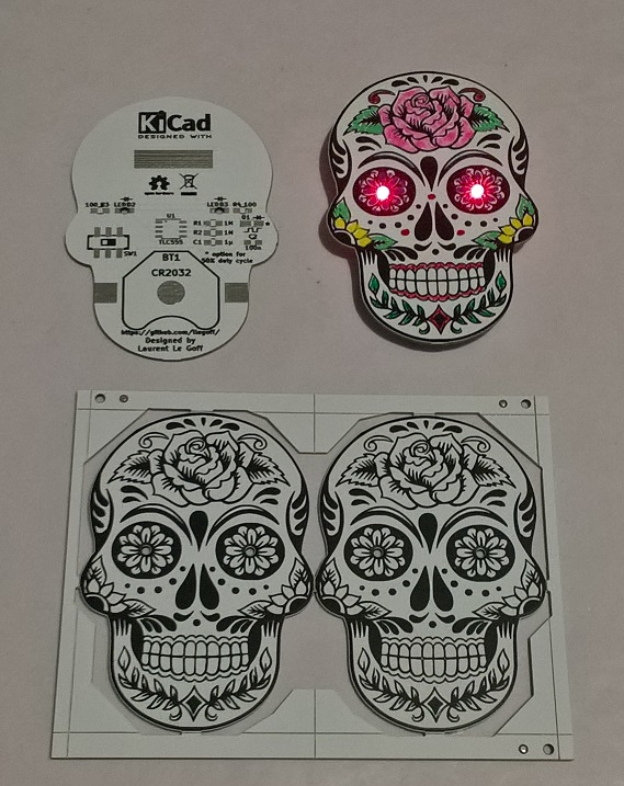
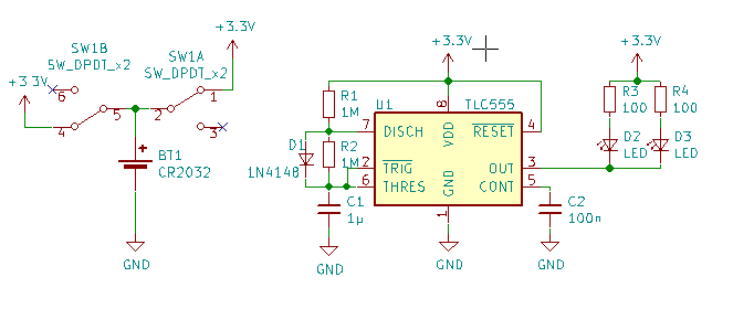
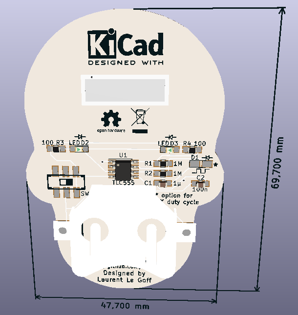
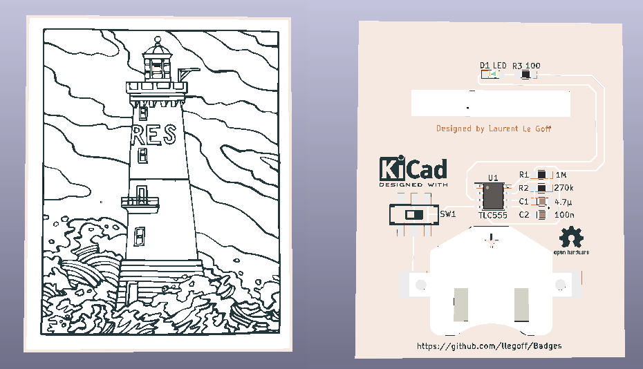
| Qty | Value | Footprint | References |
|---|---|---|---|
| 4 | 100 | Resistors_SMD:R_0805_HandSoldering | R3, R3, R4, R4 |
| 4 | 1M | Resistors_SMD:R_0805_HandSoldering | R1, R1, R2, R2 |
| 4 | LED | LEDs:LED_0805_HandSoldering | D2, D2, D3, D3 |
| 2 | _LaurentPerso:calavera | , | |
| 2 | 100n | Capacitors_SMD:C_0805_HandSoldering | C2, C2 |
| 2 | 1N4148 | Diodes_SMD:D_MicroMELF_Hadsoldering | D1, D1 |
| 2 | 1µ | Capacitors_SMD:C_0805_HandSoldering | C1, C1 |
| 2 | CR2032 | _LaurentPerso:CR2032_smd | BT1, BT1 |
| 2 | SW_DPDT_x2 | _LaurentPerso:SW_DPDT_MSS22D18 | SW1, SW1 |
| 2 | TLC555 | Housings_SOIC:SOIC-8_3.9x4.9mm_Pitch1.27mm | U1, U1 |
The 26 most common of 32 parts.


adam-kabbara/RSX-CANSAT-2026
This is a repository design to manage the files made by the Aerial team under the Robotics for Space eXploration design team at the University of Toronto

bastian-bou/NixieNTPClock
Nixie clock around ESP32 connected to a NTP server

johnbeardmore/oBeMS
Open source environmental monitoring, automatic meter reading and building management system.

MichMich/555MonoStableRelay
A 555 timer controlled mono stable relay designed in KiCad.

SolderedElectronics/Capacitive-soil-sensor-hardware-design
Hardware design, BOM, gerbers and 3D files for Capacitive-soil-sensor designed by Soldered Electronics.


AdventurousProgrammer/SeniorDesignPCB
This is the Diwali Light Chaser PCB For Senior Design
It measures 110 × 90 mm and has 2 copper layers, 1.6 mm thick.
32 parts, built around the TLC555N and CR2032. The full list of its parts is on this page, with links to each part's symbol and footprint where PCBKit's library has them.
From the llegoff/Badges repository on GitHub, at the commit this page was made from: the board is calavera/panel.kicad_pcb. PCBKit opens the board in the browser, with nothing to install.
Its repository states no licence, so its author keeps all rights: ask llegoff before reusing the design.

